News Posts matching #300 mm wafer

Return to Keyword Browsing

TSMC Celebrates 30th North America Technology Symposium with Innovations Powering AI with Silicon Leadership

TSMC today unveiled its newest semiconductor process, advanced packaging, and 3D IC technologies for powering the next generation of AI innovations with silicon leadership at the Company's 2024 North America Technology Symposium. TSMC debuted the TSMC A16 technology, featuring leading nanosheet transistors with innovative backside power rail solution for production in 2026, bringing greatly improved logic density and performance. TSMC also introduced its System-on-Wafer (TSMC-SoW) technology, an innovative solution to bring revolutionary performance to the wafer level in addressing the future AI requirements for hyperscaler datacenters.

This year marks the 30th anniversary of TSMC's North America Technology Symposium, and more than 2,000 attended the event, growing from less than 100 attendees 30 years ago. The North America Technology Symposium in Santa Clara, California kicks off TSMC Technology Symposiums around the world in the coming months. The symposium also features an "Innovation Zone," designed to highlight the technology achievements of our emerging start-up customers.

MICLEDI Microdisplays Raises Series A Funding to Advance Best-in-Class microLED Display Design and Manufacturing

MICLEDI Microdisplays today announced a first closing of its Series A funding round with participation from imec.xpand, PMV, imec, KBC and SFPIM demonstrating strong support for the company's value proposition and commercial and technological progress achieved in the seed round. Series A follows a significant seed round award and additional non-dilutive funding in the form of grants and other vehicles from VLAIO. This brings the company's total funding to date to nearly $30 million.

"The company's achievements during this seed round have been astounding," said Sean Lord, CEO of MICLEDI. "Our door is open to engagements with some of the world's largest and most innovative electronic product manufacturing companies, most of whom are working on their own internal development projects for augmented reality (AR) displays in such diverse use cases as smart-wearable devices and automotive HUDs. This level of total funding to date is almost unheard of for a four-year-old startup."

TSMC to Open Kumamoto Fab 1 on February 24, Fab 2 to Begin Operations in 2027

Taiwan Semiconductor Manufacturing Company (TSMC) is set to open its new semiconductor fabrication plant in Kumamoto Prefecture, Japan, on February 24. This facility, known as Japan Advanced Semiconductor Manufacturing (JASM), represents a significant milestone for Japan's semiconductor industry. JASM spans 52 hectares and is designed to produce mature 40, 22/28, and 12/16 nm fabrication technologies in the Fab 1. The Fab 1 has an initial monthly capacity of 40,000 300 mm wafers, scalable to 50,000 wafers per month in the near term. However, TSMC is set to expand the Kumamoto facility with Fab 2, which will produce 7 nm and 6 nm nodes and is scheduled to begin operations at the end of the 2027 calendar year. The Japanese government is set to subsidize the Fab 2 expansion with around $5 billion in aid. Combining Fab 1 and Fab 2, the JASM Kumamoto facility could produce 100,000 300 mm wafers per month once the production of Fab 2 starts. According to market research firm TrendForce, JASM provides significant additional capacity for TSMC amid a global chip shortage. It also boosts Japan's domestic chipmaking capabilities, reducing reliance on imports.

JASM is the first brand-new foreign-operated fab built in Japan. The Japanese government provided grants and tax breaks to incentivize Kumamoto Fab 1 construction as part of a national strategy to re-shore more semiconductor production and is now doing it again with Fab 2. TSMC also received subsidies from customers like Sony, SSS, DENSO and Toyota. Dr. CC Wei, CEO of TSMC, stated that JASM will "shape Japan's semiconductor landscape over the next decade." TrendForce analysts echo this sentiment, noting that JASM's advanced nodes will enable cutting-edge chip designs from Japanese automotive and consumer electronics brands. The inauguration ceremony on February 24 will be attended by TSMC partners, customers, and government representatives. JASM is expected to ramp up production over the coming year. TSMC has other non-Taiwan investments, like the facility in construction in Phoenix, Arizona, which will start mass production of chips by the end of 2027 or early 2028. At that point, the global semiconductor capacity constraints will ease significantly.
TSCM JASM

Texas Instruments Breaks Ground on New 300-mm Semiconductor Wafer Fabrication Plant in Utah

Texas Instruments (TI) today broke ground on its new 300-mm semiconductor wafer fabrication plant (or "fab") in Lehi, Utah. Joined by Utah Governor Spencer Cox, state and local elected officials, as well as community leaders, TI President and Chief Executive Officer Haviv Ilan celebrated the first steps toward construction of the new fab, LFAB2, which will connect to the company's existing 300-mm wafer fab in Lehi. Once completed, TI's two Utah fabs will manufacture tens of millions of analog and embedded processing chips every day at full production.

"Today we take an important step in our company's journey to expand our manufacturing footprint in Utah. This new fab is part of our long-term, 300-mm manufacturing roadmap to build the capacity our customers will need for decades to come," said Ilan. "At TI, our passion is to create a better world by making electronics more affordable through semiconductors. We are proud to be a growing member of the Utah community, and to manufacture analog and embedded processing semiconductors that are vital for nearly every type of electronic system today."

STMicroelectronics and GlobalFoundries to advance FD-SOI ecosystem with new 300mm manufacturing facility in France

STMicroelectronics, a global semiconductor leader serving customers across the spectrum of electronics applications, and GlobalFoundries Inc., a global leader in feature-rich semiconductor manufacturing, today announced they have signed a Memorandum of Understanding to create a new, jointly-operated 300 mm semiconductor manufacturing facility adjacent to ST's existing 300 mm facility in Crolles, France. This facility is targeted to ramp at full capacity by 2026, with up to 620,000 300 mm wafer per year production at full build-out (~42% ST and ~58% GF).

ST and GF are committed to building capacity for their European and global customer base. This new facility will support several technologies, in particular FD-SOI-based technologies, and will cover multiple variants. This includes GF's market leading FDX technology and ST's comprehensive technology roadmap down to 18 nm, which are expected to remain in high demand for Automotive, IoT, and Mobile applications for the next few decades. FD-SOI technology has origins in the Grenoble (France) area. It has been part of ST technology and product roadmap in its Crolles facility since the early beginnings, and it was later enabled with differentiation and commercialized for manufacturing at GF's Dresden facility. FD-SOI offers substantial benefits for designers and customers, including ultra-low power consumption as well as easier integration of additional features such as RF connectivity, mmWave and security.

Intel Breakthroughs Propel Moore's Law Beyond 2025

In its relentless pursuit of Moore's Law, Intel is unveiling key packaging, transistor and quantum physics breakthroughs fundamental to advancing and accelerating computing well into the next decade. At IEEE International Electron Devices Meeting (IEDM) 2021, Intel outlined its path toward more than 10x interconnect density improvement in packaging with hybrid bonding, 30% to 50% area improvement in transistor scaling, major breakthroughs in new power and memory technologies, and new concepts in physics that may one day revolutionize computing.

"At Intel, the research and innovation necessary for advancing Moore's Law never stops. Our Components Research Group is sharing key research breakthroughs at IEDM 2021 in bringing revolutionary process and packaging technologies to meet the insatiable demand for powerful computing that our industry and society depend on. This is the result of our best scientists' and engineers' tireless work. They continue to be at the forefront of innovations for continuing Moore's Law," said Robert Chau, Intel Senior Fellow and general manager of Components Research.

Infineon's New 300 mm Fab Opens Three Months Ahead of Schedule

Finally some good news from the semiconductor industry, Infineon has announced the opening of its new €1.6 billion, 300 mm, or 12-inch wafer semiconductor factory. That said, we're somewhat confused with the press release, as it states that "the chips are manufactured on 300-millimeter thin wafers, which at 40 micrometers are thinner than a human hair" and that Infineon is a "global pioneer in 300-millimeter thin-wafer technology". This is why you need someone to proofread press releases before distributing them.

Anyhow, back on topic. The fab has nearly 60,000 square meters of gross floor space and production will be ramped up over the next four to five years, so it's not going to alleviate the current chip shortage any time soon. The fab is located in Villach, Austria and has taken three years to build. The first wafers produced in the fab are said to be leaving it this week and although Infineon didn't specify what chips they'll end up as, the fab is set up to initially cater for the automotive industry, data centers and the renewable energy industry.

Bosch Unveils One Billion Euro Chip Manufacturing Facility in Germany

Robert Bosch GmbH, commonly known as just Bosch, has today unveiled the results of the company's biggest investment ever. On Monday, the company has unveiled its one billion Euro manufacturing facility, which roughly translates to 1.2 billion US Dollars. The manufacturing plant is located in Dresden, Germany, and it aims to supply the leading self-driving automobile companies with chips that are in great demand. As the main goal for the plant is to manufacture chips for the automotive industry, this new 7,200 m² Dresden facility is supposed to provide car makers with Application-Specific Integrated Circuits (ASICs) for power management and tasks such as triggering the automatic braking system of cars.

The one billion Euro facility was funded partly by the funds coming from the European Union investment scheme, which donated as much as 200 million Euros ($243 million). The goal of the plan is to start with the manufacturing of chips for power tools as early as July and start production of automotive chips in September. All of the chips will be manufactured on 300 mm wafers, which offers a major improvement in quantity compared to 200 and 150 mm wafers currently used by Bosch. The opening of this facility will surely help with the global chip shortages, which have even hit the automotive sector.

GLOBALFOUNDRIES and GlobalWafers Partnering to Expand Semiconductor Wafer Supply

GLOBALFOUNDRIES (GF ), the global leader in feature-rich semiconductor manufacturing, and GlobalWafers Co., Ltd. (GWC), one of the top silicon wafer manufacturers in the world, today announced an $800 million agreement to add 300 mm silicon-on-insulator (SOI) wafer manufacturing and expand existing 200 mm SOI wafer production at GWC's MEMC facility in O'Fallon, Missouri.

The silicon wafers produced by GWC are key input materials for semiconductors and an integral part of GF's supply chain. The wafers are used in GF's multi-billion dollar manufacturing facilities, or fabs, where they are used to manufacture the computer chips that are pervasive and vital to the global economy. Today's announcement expands GF's domestic silicon wafer supply from the United States.

UMC Investing $3.6 billion on 28 nm Manufacturing Capabilities Amidst Worldwide Semiconductor Shortages

UMC has announced plans to invest $3.6 billion in increasing output from its 28 nm manufacturing facilities. This move comes amidst a global semiconductor shortage, and isn't the first time a semiconductor manufacturer "dust off" their older manufacturing processes as a way to remove pressure from more modern silicon manufacturing capabilities. In this case, UMC will be increasing manufacturing output from its 300 mm Fab 12A facility in Tainan, Taiwan.

UMC has entered agreements with some of its clients, who will be paying upfront for expected chip rollout in the future. In exchange, clients will get the benefits of preset pricing (thus avoiding any potential increases arising from increased demand or general price fluctuation), as well as UMC's assurance of certain manufacturing volume allocation towards their needs. Fab 12A currently manufactures 90,000 300 mm wafers per month (wpm). An additional 10,000 wpm is being installed this year and phase six will add another 27,500 wpm to the mix. The mature 28 nm tools will be installed in floors that already feature support for future tooling upgrades to 14 nm. UMC expects to hire around 1,000 additional employees as part of this expansion effort.

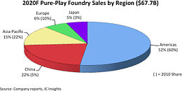
China Forecast to Represent 22% of the Foundry Market in 2020, says IC Insights

IC Insights recently released its September Update to the 2020 McClean Report that presented the second of a two-part analysis on the global IC foundry industry and included a look at the pure-play foundry market by region.

China was responsible for essentially all of the total pure-play foundry market increase in 2018. In 2019, the U.S./China trade war slowed China's economic growth but its foundry marketshare still increased by two percentage points to 21%. Moreover, despite the Covid-19 shutdown of China's economy earlier this year, China's share of the pure-play foundry market is forecast to be 22% in 2020, 17 percentage points greater than it registered in 2010 (Figure 1).

GLOBALFOUNDRIES Ceases Operations in its Chengdu Fab

GLOBALFOUNDRIES ceased all operations in its joint-venture fab in Chengdu, China. The fab opened its doors in 2018, and was supposed to mass-produce 300 mm wafers on the 22FDX technology in a 65,000 square meter facility. The company's Chinese partner, the Chengdu Municipality, had at the time boasted of investments into the fab peaking at $10 billion. The two had also announced $2 billion in initial design wins.

GloFo's announcement to cease operations and possibly withdraw from Chengdu comes hot on the heals of a separate announcement bolstering its mainland US based facilities up to US-DoD specs for secure manufacturing, a sign that the company will scale up investment into US-based facilities. GloFo's foreshadowed withdrawal from manufacturing in China is part of the ongoing "tech war" between the US and China, with the US getting American (and West-aligned) tech companies to pull manufacturing out of China, the biggest casualties of which is Huawei.

Toshiba and Western Digital Readying 128-layer 3D NAND Flash

Toshiba and its strategic ally Western Digital are readying a high-density 128-layer 3D NAND flash memory. In Toshiba's nomenclature, the chip will be named BiCS-5. Interestingly, despite the spatial density, the chip will implement TLC (3 bits per cell), and not the newer QLC (4 bits per cell). This is probably because NAND flash makers are still spooked about the low yields of QLC chips. Regardless, the chip has a data density of 512 Gb. With 33% more capacity than 96-layer chips, the new 128-layer chips could hit commercial production in 2020-21.

The BiCS-5 chip reportedly features a 4-plane design. Its die is divided into four sections, or planes, which can each be independently accessed; as opposed to BiCS-4 chips that use a 2-plane layout. This reportedly doubles the write performance per unit-channel to 132 MB/s from 66 MB/s. The die also reportedly uses CuA (circuitry under array), a design innovation in which logic circuitry is located in the bottom-most "layer," with data layers stacked above, resulting in 15 percent die-size savings. Aaron Rakers, a high-technology industry market analyst with Wells Fargo, estimates that Toshiba-WD's yields per 300 mm wafer could be as high as 85 percent.

TSMC Fab 14 B Hit With Chemical Contamination; NVIDIA, MEDIATEK, Huawei, Hisilicon Lines Affected

TSMC's Fab 14 B has been affected with a chemical contamination that has put a considerable number of wafers in suspend mode. Fab 14 B essentially produces 12 and 16 nm, 300 mm wafers for 14 companies, including NVIDIA, MEDIATEK, Huawei and Hisilicon. Reportedly, between 10,000 and 30,000 wafers have been affected (though not scrapped, so there might be salvageable bits and pieces here and there). Of course, every wafer will have to go through a thorough certification process, and the fab will have to go down for the company to purge any remains of these botched chemical compounds.

To put things into perspective, though, Fab 14 B is one of TSMC's Gigafabs, which have a rated monthly output of 100k wafers - so production worth between three and ten days could be affected already, with the additional downtime accruing lost potential fabrication. This event isn't expected to significantly affect availability of any of the products for any of the companies, but these are becoming, at the very least, late inventory - this could well play into some speculative increases in pricing from some players in the market.

Q4 2017 300 mm Silicon Wafer Pricing to Increase 20% YoY in DRAM-like Squeeze

Silicon wafers are definitely the best kind of wafers for us tech enthusiasts, but as we all know, required financial resources for the development and production of these is among the most intensive in development costs and R&D. It's not just about the cost of employing enough (and crucially, good enough) engineers that can employ the right tools and knowledge to design the processing miracles that are etched onto wafers; there's also the cost of good, old production as well. Extreme Ultraviolet Lithography Systems that are used for the production of silicon wafers are about the size of a city bus, and typically cost more than 100 million euros ($115.3 million) each. ASML, a Dutch company that specializes in this kind of equipment, announced this year it was expecting to see a 25% revenue growth for 2017. Increased demand for these systems - and added cost of development of ever increasingly small and complex etchings in wafers - means this sector is seeing strong growth. But where there is strong growth, there is usually high demand, and high demand means higher strain on supply, which may sometimes not be able to keep up with the market's needs.

This is seemingly the case for wafer pricing; as demand for wafer production has been increasing, so to are prices. Faced with increased demand, companies are usually faced with a tough question to answer in regards to the correct course of action. Usually, it goes like this: higher demand at the same supply level means higher pricing. However, if supply isn't enough to satisfy demand, manufacturers are losing out on potential increased sales. This leads most companies to increase supply relative to demand, but always with lower projected output than demand requires, so they can bask in both increased ASP (Average Sale Price) and higher number of sales. This has been the case with DRAM memory production for some time now: and is happening with 300 mm silicon wafers as well.
Return to Keyword Browsing
May 19th, 2024 23:59 EDT change timezone

New Forum Posts

Popular Reviews

Controversial News Posts