Thursday, January 7th 2010

NVIDIA GF100 Graphics Card Chugs Along at CES

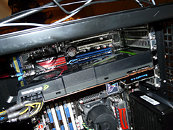
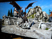
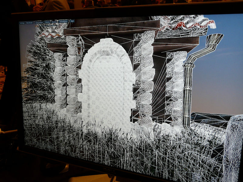
NVIDIA's next generation graphics card based on the Fermi architecture, whose consumer variant is internally referred to as GF100 got to business at the CES event being held in Las Vegas, USA, performing live demonstration of its capabilities. The demo PC is housing one such accelerator which resembles the card in past sightings. Therefore it is safe to assume this is what the reference NVIDIA design of GF100 would look like. The accelerator draws power from 6-pin and 8-pin power connectors. It has no noticeable back-plate, a black PCB, and a cooler shroud with typical NVIDIA styling. The demo rig was seen running Unigine Heaven in a loop showing off the card's advanced tessellation capabilities in DirectX 11 mode. The most recent report suggests that its market availability can be expected in March, later this year. No performance figures have been made public as yet.
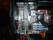
A short video clip after the break.

Source: PCWatch
Add your own comment

105 Comments on NVIDIA GF100 Graphics Card Chugs Along at CES

#1
3volvedcombat
This is good very good. Im sitting here staring at my GTX 260's wondering if they should go on the [FS] forum because of the proof Ive just seen.
Posted on Reply
#2
Imsochobo
wondering if those at nvidia's marketing team uses 3 years to choose what kind of breakfast they are going to buy.

Because their naming schemes change every year....

So is GF100 entry ? best? lowend.... uhm ?

Gj getting something to show this round Nvidia!
Posted on Reply
#3
btarunr
Editor & Senior Moderator
Imsochobowondering if those at nvidia's marketing team uses 3 years to choose what kind of breakfast they are going to buy.

Because their naming schemes change every year....
GF100 is an internal codename. Terms like G92, GT200, or GF100, aren't meant to be marketing names anyway.
Posted on Reply
#4
Imsochobo
btarunrGF100 is an internal codename. Terms like G92, GT200, or GF100, aren't meant to be marketing names anyway.
ohh.

well then they had issues finding internal codenames then :P
Posted on Reply
#5
Airbrushkid
Why? you'll still have to wait til March. I have as follows -

TNT-2
Geforce 3
Geforce 5600
Geforce 6600 gt
Geforce 6800 OC
Geforce 8600 gts
Geforce 8800 gts 320
Geforce 9800 gt 1 gig
GTX 260 216
GTX 285 SSC

No plans on selling. When the new card comes out I may buy.
3volvedcombatThis is good very good. Im sitting here staring at my GTX 260's wondering if they should go on the [FS] forum because of the proof Ive just seen.
Posted on Reply
#6
BUCK NASTY
4P Enthusiust
3volvedcombatThis is good very good. Im sitting here staring at my GTX 260's wondering if they should go on the [FS] forum because of the proof Ive just seen.
They should get bumped to the dedicated folding rig;).
Posted on Reply
#7
btarunr
Editor & Senior Moderator
Imsochoboohh.

well then they had issues finding internal codenames then :P
Codenames aren't meant for consumers anyway. They won't feature on specs sheets or boxes. Hence they can call their stuff whatever they want to, and that would still be a non-issue to the consumer.
Posted on Reply
#8
cadaveca
My name is Dave
Anyone else notice that it looks like they got 3x pci-e connector wires going to 2x the pci-e plugs?(note the number of yellow 12v wires):wtf: Something is fishy here...
Posted on Reply
#9
btarunr
Editor & Senior Moderator
cadavecaAnyone else notice that it looks like they got 3x pci-e connector wires going to 2x the pci-e plugs?(note the number of yellow 12v wires):wtf: Something is fishy here...
No, nothing fishy.


The 8-pin connector is an internode (a single line, in the middle of which is a connector).
Posted on Reply
#10
AlCabone
AirbrushkidWhy? you'll still have to wait til March. I have as follows -

TNT-2
Geforce 3
Geforce 5600
Geforce 6600 gt
Geforce 6800 OC
Geforce 8600 gts
Geforce 8800 gts 320
Geforce 9800 gt 1 gig
GTX 260 216
GTX 285 SSC

No plans on selling. When the new card comes out I may buy.
Do you actually use all of those?
Posted on Reply
#11
cadaveca
My name is Dave
btarunrNo, nothing fishy.

img.techpowerup.org/100107/btalkjhas37.jpg

The 8-pin connector is an internode (a single line, in the middle of which is a connector).
If you say so. Just seems ot me this is one of the early samples, and has high power draw. 8-pin power only requires 3x 12v wires, not 6, as is shown.

No big deal..jsut means maybe production cards will be better/faster.

but yeah, I hear what you are saying...from 8-pin, a 6-pin hangs. But then why didn't they use just the single cable?

Good idea of length here too...that's a Raven RV01 case.
Posted on Reply
#13
btarunr
Editor & Senior Moderator
cadavecaIf you say so. Just seems ot me this is one of the early samples, and has high power draw. 8-pin power only requires 3x 12v wires, not 6, as is shown.

No big deal..jsut means maybe production cards will be better/faster.

but yeah, I hear what you are saying...from 8-pin, a 6-pin hangs. But then why didn't they use just the single cable?


Capiche?

It's just the way the PSU's cables were designed. The "second" connector in the diagram above is what went into the card in the picture above. There's nothing more to it than this.
Posted on Reply
#14
cadaveca
My name is Dave
Capisco!!

Again, then why didn't they use just the single cable?
Posted on Reply
#15
btarunr
Editor & Senior Moderator
cadavecaCapisco!!

Again, then why didn't they use just the single cable?
It does not make a difference.
Posted on Reply
#16
cadaveca
My name is Dave
To me, it does, dependant on the PSU used.


Meh...just something to talk about...:laugh:...clearly this is not a full production card, as there are a few months left, almost, until release.
Posted on Reply
#17
btarunr
Editor & Senior Moderator
cadavecaTo me, it does, dependant on the PSU used.
I'll say it again, it does not make a difference. Besides they are not doing a performance evaluation there, so there's no scope to even speculate on something this trivial.
Posted on Reply
#18
yogurt_21
interesting being that there were some rumors regarding the tessalation capabilities.

@ the naming scheme I think this is supposed to be the 10th rendition of the geforce series hence the gf on the tag, which means they are more than likely countign the gt200 as the geforce 9 onmiting the 9800's as the g92 first bore an 8800 designation.

it likly means nvidia is returnign to a normal card progression internal naming scheme.

speculation truly especially by cores without revision series were only up to 6 on the gt200 which would make the gf100 the 7th.
Posted on Reply
#19
Benetanegia
cadavecaCapisco!!

Again, then why didn't they use just the single cable?
Probably just for better cable mangement. I've done that with some of my cables.

Tom's Hardware on Fermi - www.tomshardware.com/reviews/ces-2010-fermi,2527-4.html
Fermi Graphics: Really? Really!

I was just about to leave the event when Ken Brown, Nvidia PR guy (not to mention former executive editor of Computer Gaming World back in the day), tapped me on the shoulder and asked me if I wanted to see a Fermi-based GPU.

Fermi is Nvidia’s massive re-imagining of its architecture with a strong emphasis on GPU computing capabilities. It’s still very much a graphics design, but the gestation period for the first Fermi chips has been a long and painful one. Nick Stam at Nvidia showed off the new GPU running inside an X58-based Core i7 system.

The card overhung an ATX motherboard slightly, but Stam noted that the cooler wasn’t final hardware, and clocks and other specs weren't ready to be announced yet. The system was running the Uniengine DirectX 11 benchmark, and Nick insisted that the results were already better than AMD’s fastest GPU. Nick was also noncommittal about power consumption, but the card looked to be using both 8-pin and 6-pin PCIe power connectors. Since it wasn’t final hardware, though, it’s uncertain as to what will show up when retail cards emerge.

Nick also insisted that GF100 (that’s the code name, not the product name) would be a "Q1 product." So we’ll just have to wait and see. But after all the delays and silence from Nvidia, Fermi-based graphics is starting to look real.
He's claiming Fermi to be faster than HD5970 and that's from a Nvidia guy this time. Real or not, it's one step closer to being an official statement, not rumors or fakes (now, they really were fakes?). I'll chose to believe him, because some months ago I made my own calculations based on the specs and reached that conclusion, as some of you may remember. We'll see, but I'm optimistic.
Posted on Reply
#20
Imsochobo
btarunrCodenames aren't meant for consumers anyway. They won't feature on specs sheets or boxes. Hence they can call their stuff whatever they want to, and that would still be a non-issue to the consumer.
i was joking around :P

As my head gets dizzy by knowing whats what.

And now it seems ati is doing the same, still not as hard as nvidia's naming have been lately, but they have started so they might follow footsteps :P
Posted on Reply
#21
Animalpak
whoooo nice, things comes real this time
Posted on Reply
#22
HalfAHertz
Finally! May the price wars commence!
Posted on Reply
#23
phanbuey
price wars... mmm price wars. Can't wait.
Posted on Reply
#24
20mmrain
I too thought it looked like 3 wires at first until I looked again. It is only two 1 6pin + 1 8 pin. Just must be the way they had the wires situated.

Also did anyone notice that the guy running the demo happened to keep switching the modes during the really intense tessellation parts? It was either him doing it or that is the way they had it set up to run.
I the parts that it did run with full Tessellation it did look a little choppy at times. I do think that it looked a little smoother than my single 5870..... but not too much. Not enough to make me really impressed.

So let's say for a second that this thing really does beat a 5870 by 36%. Well I wouldn't be surprised it only is coming out half a year later. If you ask me that number wouldn't be that impressive for 6 months later.

But I still like the idea of the technology that they are using. I also think it will be a great addition to the world of GPU's. It will keep things moving forward that is for sure!

But If I was that confident with it's performance and I were Nvidia. I would have left the FPS counter on the bottom and the top..... still left out there for all to see. But they didn't makes me wonder.
Posted on Reply
#25
erocker
*
20mmrainI too thought it looked like 3 wires at first until I looked again. It is only two 1 6pin + 1 8 pin. Just must be the way they had the wires situated.

Also did anyone notice that the guy running the demo happened to keep switching the modes during the really intense tessellation parts? It was either him doing it or that is the way they had it set up to run.
I the parts that it did run with full Tessellation it did look a little choppy at times. I do think that it looked a little smoother than my single 5870..... but not too much. Not enough to make me really impressed.

So let's say for a second that this thing really does beat a 5870 by 36%. Well I wouldn't be surprised it only is coming out half a year later. If you ask me that number wouldn't be that impressive for 6 months later.

But I still like the idea of the technology that they are using. I also think it will be a great addition to the world of GPU's. It will keep things moving forward that is for sure!

But If I was that confident with it's performance and I were Nvidia. I would have left the FPS counter on the bottom and the top..... still left out there for all to see. But they didn't makes me wonder.
I don't know. If the card really beats a 5870 by 36%. Wouldn't Nvidia be touting it left and right? I'm hoping to see some concrete numbers by the end of CES. Really, we aren't seeing much that we haven't already seen.
Posted on Reply
Add your own comment
Apr 16th, 2024 13:56 EDT change timezone

New Forum Posts

Popular Reviews

Controversial News Posts