Wednesday, April 21st 2010

Intel Sandy Bridge to Introduce New Sockets, Chipsets, Reorganize Platform Further
Intel plans a pair of new sockets for launch with its new processor architecture that succeeds Westmere, codenamed "Sandy Bridge", which are due for 2011. As part of its "tick-tock" product launch strategy, the company is currently transitioning between the 45 nm "tock" (Nehalem architecture), and 32 nm "tick" (Westmere architecture). In 2011, it will transition from the 32 nm "tick" (Westmere architecture), to the 32 nm "tock" (Sandy Bridge architecture). The company uses a "tick-tock" model of process development, where each processor architecture gets to be made in two successive manufacturing processes, while each process gets to build two succeeding architectures. It seems to have become clear that with Sandy Bridge, Intel will also switch to new socket designs, making existing motherboards obsolete then. Architecturally, Sandy Bridge will introduce new feature-sets that make the CPU more powerful, clock-to-clock, such as AVX - Advanced Vector Extensions, an evolution of the SSE instruction set, native AES engine which has been introduced with Westmere, and so on.
The present LGA-1156 package on which Intel builds value-through-performance processors including a bulk of mainstream processors, will be succeeded with the LGA-1155 package. Though similar, LGA-1155 and LGA-1156 are not inter-compatible, meaning that LGA-1155 processors will not work on existing LGA-1156 motherboards, and LGA-1156 processors will not work on LGA-1155 motherboards, either. For these processors, the arrangement of vital components is similar to the LGA-1156 package, except that every LGA-1155 processor - dual-core or quad-core - will feature an on-die display controller. The die itself will be monolithic, where the northbridge component completely integrates with the processor component, leaving only the southbridge outside the package, on the motherboard. Currently, the "Clarkdale" and "Arrandale" dual-core processors have the processor and northbridge components on separate dies, but on the same package. LGA-1155 is also designated as socket H2 (LGA-1156 is H1), the package is identical in size to LGA-1156, but has a different pin layout and orientation notch.
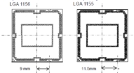
Chipsets that drive the LGA-1156 platform include P67, H67, H61, and Q67, which will support features which were conceived prior to Ibex Peak platform's launch, but were shelved, such as ONFI NAND Flash "Braidwood", etc. USB 3.0 still isn't part of the feature-set, though native SATA 6 Gb/s support is on the cards.
The next big platform to succeed the LGA-1366, which caters to processors in the upper performance-though-enthusiast segments is the "Patsburg" platform, succeeding the existing "Tylersburg" based Intel X58, 5000 series chipsets. Here, Intel will introduce a massive new socket, the LGA-2011. The pin count is drastically increased for two reasons: the processor will have a 256-bit wide memory interface (quad-channel DDR3), and the northbridge component (currently X58 PCH) will be integrated completely into the processor package, upping the pin count with the PCI-Express and DMI pins. The on-die PCI-Express 2.0 root-complex will give out 32 lanes for graphics (unlike 16 lanes on the LGA-1155), and a DMI link to the so-called "Intel X68" chipset, which is relegated to being a Platform Controller Hub, just like the P55, or P67. The X68 could have a feature-set similar to the P67.
Source:
bit-tech.net
The present LGA-1156 package on which Intel builds value-through-performance processors including a bulk of mainstream processors, will be succeeded with the LGA-1155 package. Though similar, LGA-1155 and LGA-1156 are not inter-compatible, meaning that LGA-1155 processors will not work on existing LGA-1156 motherboards, and LGA-1156 processors will not work on LGA-1155 motherboards, either. For these processors, the arrangement of vital components is similar to the LGA-1156 package, except that every LGA-1155 processor - dual-core or quad-core - will feature an on-die display controller.


The next big platform to succeed the LGA-1366, which caters to processors in the upper performance-though-enthusiast segments is the "Patsburg" platform, succeeding the existing "Tylersburg" based Intel X58, 5000 series chipsets. Here, Intel will introduce a massive new socket, the LGA-2011. The pin count is drastically increased for two reasons: the processor will have a 256-bit wide memory interface (quad-channel DDR3), and the northbridge component (currently X58 PCH) will be integrated completely into the processor package, upping the pin count with the PCI-Express and DMI pins. The on-die PCI-Express 2.0 root-complex will give out 32 lanes for graphics (unlike 16 lanes on the LGA-1155), and a DMI link to the so-called "Intel X68" chipset, which is relegated to being a Platform Controller Hub, just like the P55, or P67. The X68 could have a feature-set similar to the P67.
119 Comments on Intel Sandy Bridge to Introduce New Sockets, Chipsets, Reorganize Platform Further
I agree that it was bound to happen. Once 32nm CPUs were released, they were only released on 1156, and their integrated GPUs only worked on P57 boards, which there were very few of.
Never mind that they end up pissing off their buyers, especially the enthusiasts.
Besides from techies how many people actually upgrade the CPU in their computer?? I'd like to table a guess of much less than 1%.
So why would Intel not change their sockets to accommodate their latest in technology?
You should be used to it by now. Otherwise, switch to AMD.
I hate to admit it, and it leaves me feeling a little burnt, but the truth is, it doesn't really effect me that much.
B - MATX format is too small
maybe they can sort it cause X68 is just one chip, but, its just too much.
i'm still going to get an i7 processor and mobo sometime this year why ?
well i haven't upgraded in about 7 years :eek::wtf::shadedshu so hopefully the new i7
will last just as long as my current system has, which by then there might be a 24 core processor out
that will :nutkick: my eyes brain and wallet:laugh::D