Friday, July 23rd 2010

NVIDIA GF106 Reference PCB Drawings Surface
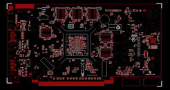
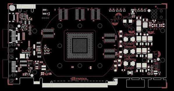
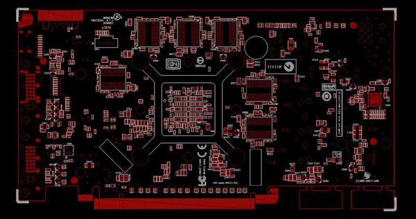
Two days after reports surfaced about NVIDIA readying the GeForce GTS 450 mainstream graphics SKU for a late August launch, PCInLife got a hold of the PCB's x-ray drawings, which reveals quite a bit about the GF106 GPU the GTS 450 is based on. The PCB reveals a square GPU that is bordered on three sides with six memory chips, is powered by a 3+1 phase VRM, draws power from a 6-pin PCI-E power input, supports 2-way SLI, and has display outputs including two DVI and a mini-HDMI.
The presence of six memory chips particularly intrigues, as it could indicate a 192-bit wide memory interface. Perhaps two of those slots are empty, if GTS 450 does end up with a 128-bit memory interface, and enabled on a higher SKU, or that GTS 450 itself has a 192-bit memory interface (supporting 768 MB or 1536 MB of GDDR5 memory). Expect more details to come out in the run up for end-August.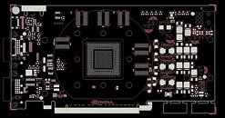
Source:
PCinLife
The presence of six memory chips particularly intrigues, as it could indicate a 192-bit wide memory interface. Perhaps two of those slots are empty, if GTS 450 does end up with a 128-bit memory interface, and enabled on a higher SKU, or that GTS 450 itself has a 192-bit memory interface (supporting 768 MB or 1536 MB of GDDR5 memory). Expect more details to come out in the run up for end-August.
13 Comments on NVIDIA GF106 Reference PCB Drawings Surface
it could mean that it will be a similar situation to the GTX460 where there are 2 cards a high end and low end one.
based on the size of the core its gotta have 240sp tops, and would only have a max of 24 rops
In any case comparing GF10x to GT200 on a pure SP count basis, is not fair, it is as unfair as it was to compare the 320 SPs in the HD2900 to the 56 "SPs" (48 pixel shaders + 8 vertex shaders) in the X1900. It is a new architecture, a completely different way of doing things.
And that not only pertains to the actual architecture and its drivers, but also to how games are programed and the actual load balance of the content (textures, shaders, filters...). Game performance for cards such as te GTX285 and the HD5000 is what it is now thanks to the accumulated optimizations, programing efforts and content customization made by game developers since the introduction of G80 and R600. That's almost 5 years of optimizations. You are not going to start seeing a similar level of optimization until the games that have been programmed with fermi in mind since the beginning start to pop up and considering game developing cycles nowadays, that means at the very least 1-2 years in the future.
EDIT: Regarding competition against the HD5770, I did some math. I think that GF106 is going to be literally half a GF100 (but with problems fixed like in GF104) anf GF108 is going to be half a GF104. That's what the PCB suggests IMO. With 256 SPs this card would perfectly match the HD5770 if clocked at same clocks as the GTX460, because as can be seen in Wizzard's reviews, the HD5770's performance is about 75% of a GTX460 and coincidentally 256 is about 75% of 336. And that's if it's clocked at 675Mhz. IMO it's going to be clocked higher than that. There's no reason not to, for various reasons.
1- Historically the fastest SKU of mainstream chip has always been clocked 25-50 Mhz higher than the high-end chip.
2- Smaller chips reach higher clocks. Further improved manufacturing process.
3- GTX460 hints at much higher clocks. There's absolutely no technical reason* for clocking the GTX460 as low as 675 Mhz, when every reviewer has been able to clock every sample they got past 800 Mhz on stock voltages and past 900 Mhz with slightly higher volts. technically, it just doesn't make sense to leave 40% OC headroom on your chip.
*I'm 100% confident that the reason that they clocked it low and that the full enabled SKU has not been released is because they would destroy the GTX470 and maybe even the GTX480 (this last one not on pure performance, but in the same way the 512MB 8800GTS made the 8800GTX odsotete). They will just wait until GF100 inventories have been depleted. They did exactly the same with G92. This way they also obtain higher yields for the time being, although they are probably binning the best chis for a future release too. Win win.
Well there's absolutely no reason to do this with GF106 since Nvidia has no cometing products there, so I'm pretty sure they would be clocked in the 725-750 Mhz range and that will make the GTS250 some 10% faster than HD5770.