Thursday, September 16th 2010

AMD ''Barts'' GPU Detailed Specifications Surface

Barely a week after pictures of AMD's "Barts" prototype surfaced, it wasn't long before a specifications sheet followed. The all-important slide from AMD's presentation to its add-in board partners made it to sections of the Chinese media. "Barts" is a successor to "Juniper", on which are based the Radeon HD 5750 and HD 5770. The specs sheet reveals that while indeed the GPU looks to be larger physically, there are other factors that make it big:

Memory Controller
Barts has a 256-bit wide memory interface, which significantly increases its pin-count, and package-size. The "Pro" and "XT" variants (which will go on to be HD 6x50 and HD 6x70, respectively), have memory clocked at 1000 MHz and 1200 MHz, respectively, so that's nearly 100% increase in memory bandwidth .

Tiny increase in SIMD count, but major restructuring
Compared to Juniper, there seems to be an increase of only 20% in stream processor count physically. The XT variant has 960 stream processors, while the Pro variant has 800. AMD specifically mentioned SIMD block count, (10 enabled for Pro, 12 enabled for XT). If you noticed the slide, it says that the GPU is based on the "Cypress Dual Engine architecture", meaning that these 10 and 12 SIMD units will be spread across two blocks of 5 (Pro) or 6 (XT) SIMDs each, just like Cypress had two blocks of 10 SIMDs each.

Other components
The Raster Operations unit (ROP) count has been doubled to 32, TMUs stand at 40 for the Pro and 48 for the XT.

The design methodology is extremely simple. Juniper-based graphics cards anyway carry 8 memory chips to meet up to memory amount requirements of 1 GB using market-popular 1 Gbit GDDR5 chips, so why not just place those 8 chips across a 256-bit wide memory interface and double the memory bandwidth. The increased ROP count, coupled with up to 20% increase in shader compute power gives Barts the competitive edge it needs to face NVIDIA's reinvigorated GeForce 400 series after the introduction of the GeForce GTX 460. As for power draw, AMD projects the Pro variant to draw less than 150W, with the XT drawing "over" 150W.

Market Positioning
AMD doesn't have huge expectations from this. It has its task cut out: to compete with the GeForce GTX 460 768 MB and 1 GB models. While memory count ROP made the cut out NVIDIA's variants, AMD's come from clock speeds and SIMD core counts. It should then become obvious what these GPUs' pricing should look like.

When?
Usually when AMD gives out such a presentation to its AIB partners, a market release is about 3 months away.
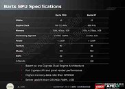
Source: ChipHell
Add your own comment

110 Comments on AMD ''Barts'' GPU Detailed Specifications Surface

#51
cheezburger
ToTTenTranzWell, this pretty much confirms the change from the old 5D shaders.
They're probably also bumping the geometry performance, namely DX11 tesselation, along with the new shaders.

Nonetheless, I have no doubt that Bart will be a whole lot smaller than GF104, thus cheaper to produce. Besides, since the HD5830 can be made with a relatively small PCB, I have no doubts this card won't be much bigger than the HD5770.


I do think they could just cut the prices in their current HD5000 line to stupidly low values (their yields should be sky-high by now) while holding off for the 32/28nm process. nVidia's underperforming Fermi architecture would allow them to do that.
i doubt they may just discontinue it rather than keep it around as there would be pointless, a card has poor shader fill rate while having more shader than new series that easily outperform it with less shader/ALU and not even playable when comes tessellation. also the die isn't much smaller/cheaper than northern islands which makes no profit at all as manufacture continues. if a barts can outperform gtx 480 while keep the price around $259~299 will make no room for evergreen. dont expecting evergreen become another g92..
20mmrainWell the thing I can't help but notice is that the 5770 has 800 stream Processors.... and this Card (supposedly the "6770") has 300 Shaders.

Now since I don't really get into the lingo of what means what.... I just know what's the most powerful at the time and how to overclock it well :)

I thought that Stream Processors was what ATI/AMD called their Shader cores correct?

If I have that right.... wouldn't this mean that this has to be new architecture? Considering that the old Stream processors were weaker then Nvidias Shader "Cuda" Cores? Now this card only has a number of 300 compared to the 5770's 800?

If I have this understood correctly.... this will be one hell of a series. We might finally be able to adjust Shader clocks on ATI cards too!? I just can't wait to see what we have instore for this generation.

I will tell you what though. Even if this card is meant to go against the GTX 460.... the DX 11 tessellation on these cards compared to Fermi (If the benchmarks are true) look like this series will leave fermi in the dust and now where to be seen.

I will definetly sell my GTX 460's for a pair of these. If not go even higher up the ladder if the price is right

That's not to mention the 960 Shader version of this card. This thing should be crazy as hell! :rockout:

But to someone out there who said that "We could see this card be on the 5870 levels" I hope so for AMD but I hope not for our sake. Because if this is the case.... we are looking at a mid card for $400 buck each and a top card for $1000 grand or more easy.
for what i know 4D format is like s core that can send 4 data in one clock, unlike previous design of 5D format that has to divided into 5 small dedicate shader pipeline. this design(4 complexity arrangement) is done by one shader core than split core to do the multiple purpose(4 simple + 1 complex format ). more like GDDR5 but it's in inside of shader core. if it's correct a shader effective data rate would be "core clock x 4" if barts's core frequency is 900mhz than the shader core will run 3.6GT(3600MT) effectively.
Posted on Reply
#52
TheLaughingMan
20mmrainWell the thing I can't help but notice is that the 5770 has 800 stream Processors.... and this Card (supposedly the "6770") has 300 Shaders.

Now since I don't really get into the lingo of what means what.... I just know what's the most powerful at the time and how to overclock it well :)

I thought that Stream Processors was what ATI/AMD called their Shader cores correct?

If I have that right.... wouldn't this mean that this has to be new architecture? Considering that the old Stream processors were weaker then Nvidias Shader "Cuda" Cores? Now this card only has a number of 300 compared to the 5770's 800?
Everything you said there about the 6770 is completely wrong and I am not sure where you got that number. They 67x0 GPU's to be released soon got double the memory bandwidth, double the ROPs (from 16 to 32), and ~20% more Streaming Processor cores for the XT.

6750 = 800 Streaming Processors 5750 = 720 Streaming Processors
6770 = 960 Streaming Processors 5770 = 800 Streaming Processors
Posted on Reply
#53
dir_d
Well if that number is correct, and they really did move this card to 4way cores that means the 5770 had 160x5 (800) stream processors and this new card will have 300x4 (1200). This card maybe be very well be 6870 and be on par with the 5870 if the numbers are correct.

edit...if the shaders still stay the same 200x4 (800) still a nice bump in performance by keeping the same number of shaders.
Posted on Reply
#54
20mmrain
TheLaughingManEverything you said there about the 6770 is completely wrong and I am not sure where you got that number. They 67x0 GPU's to be released soon got double the memory bandwidth, double the ROPs (from 16 to 32), and ~20% more Streaming Processor cores for the XT.

6750 = 800 Streaming Processors 5750 = 720 Streaming Processors
6770 = 960 Streaming Processors 5770 = 800 Streaming Processors
Oops LOL that makes much more sense Sorry it is late here and I wasn't paying that close attention.....

Here is what I saw.....


You see my cuircled red area.... on my screen it looks like 300. That is why I thought something was werid for the next level card down to go from 920 Shader to 300 shaders.

LOL goofy move on my part :banghead:

So nevermind I retract my previous ideas and statements "Blush" :p

Still on another note 32 ROP's 800 to 920 shader's 256 Bit bus..... all looks bad ass to me. Wish I could visualize more what this all meant but after looking at comparable cards and specs today. It seems what others here have been saying might be true. This card could be very close the the 5850/5870 area.
Posted on Reply
#55
cadaveca
My name is Dave
Could be that 6770 simply adds 160 more shaders, plus 256-bit bus, and there is no shader change at all. And to me, that would SUCK!!


:laugh:

Wouldn't be much faster than current 4890, with DX11 tacked on.

:eek:

Considering the "competition", there's no reason to expect more than that at all(Uh, based on cypress dual engine, each engine now has one extra cluster, hello?). New shaders might kill 470, even, if clocked high enough, so I think that might be asking to much...but boy, would it ever be nice.
Posted on Reply
#56
cheezburger
cadavecaCould be that 6770 simply adds 160 more shaders, plus 256-bit bus, and there is no shader change at all. And to me, that would SUCK!!


:laugh:

Wouldn't be much faster than current 4890, with DX11 tacked on.

:eek:

Considering the "competition", there's no reason to expect more than that at all(Uh, based on cypress dual engine, hello?). New shaders might kill 470, even, if clocked high enough, so I think that might be asking to much...but boy, would it ever be nice.
then why would amd gone this far and putting double size of rops/ram bus.....if the shader is still 5D:shadedshu
Posted on Reply
#57
cadaveca
My name is Dave
Becuase devs have been complaining about that exact thing for some time. If you go back in time, about 5 years, in my "microstutter" posts(yes, been looking at that stuff that long), texture performance(xTexture Memory Units) have been a big issue. One might even suppose that maybe this is why nv's tech excels so greatly, although math performance is much lower than AMD.

I mean, realisticlly this is what makes the most sense. I think when 32nm existed, the shader change was planned, but because they are stuck in 40nm, the changes they can make are limited...higher-order shaders are going to generate more heat in the shader core, but simply enlarging the die size, and adding more shaders, just means you need to provide better overall cooling capacity for the already existing cooler.

This is business, after all, so the biggest impact, with the smallest cost, works best. New shaders migth seem like htey'd cost less, but the dev time costs alot too. Would be far more practical to invest further time in any such changes, and make small, but effective, ones, that increase profits.
Posted on Reply
#58
Benetanegia
cheezburgerthen why would amd gone this far and putting double size of rops/ram bus.....if the shader is still 5D:shadedshu
They doubled the rops/bus width because the 5770 was already very limited. Regardless of how much more shader/texture performance the new card has 10%, 20%, 50%... a higher rop power was necessary if a tangible improvements was to be seen. AMD is commited to only use widths that are multiples of 2, instead of using intrmediate numbers like Nvidia does so that's why the 256 bit figure comes in, even though it will probably be overkill on these cards. Don't expect Cayman to have more than 256 bits. It wouldn't be the first time in history when a midrange and high-end chips share the bus width...
Posted on Reply
#59
cheezburger
BenetanegiaThey doubled the rops/bus width because the 5770 was already very limited. Regardless of how much more shader/texture performance the new card has 10%, 20%, 50%... a higher rop power was necessary if a tangible improvements was to be seen. AMD is commited to only use widths that are multiples of 2, instead of using intrmediate numbers like Nvidia does so that's why the 256 bit figure comes in, even though it will probably be overkill on these cards. Don't expect Cayman to have more than 256 bits. It wouldn't be the first time in history when a midrange and high-end chips share the bus width...
really? just few days ago some of you said barts's rops wouldn't be over 16 and stick with 128bit bus...now things change...if cayman is about twice of barts spec than that will make 64 rops....i dont think a 256bit bus can feed these rops..again things will goes different than you think...plus faster ram eats more power and runs hotter and more costly than slower ram sodont get any hope on 7gt gddr5 ram as well. because it will end up having dual 8 pin pcie on a card that's merely 32 rops/256bit bus.....

it would be historical event if both high end and main stream share the same size bus...dont tell me about g92....it's never meant to be high end if werent gt 200 delayed...

anyway just wait and see cayman's spec
Posted on Reply
#60
halfwaythere
Folks Barts is going to be the next 68xx cards. Cayman is going to be 6950 and 6970 while Antilles, the dual gpu card, will be 6990. Half this thread is filled with miss-information and people talking non-sense.

Anyways new stuff:
HD 6850 HD 5770 HD 5830 HD 5850
Codename Bart Pro XT Juniper Cypress Cypress Pro LE
Technology 40 nm 40 nm 40 nm 40 nm
Stream Proc. 1120 pcs. 800 pcs. 1120 pcs. 1440 pcs.
GPU frequency 72x MHz 850 MHz 800 MHz 725 MHz
Memory Frequency 4000 MHz 4800 MHz 4000 MHz 4000 MHz
Memory Bus 256-Bit 128-bit 256-bit 256-bit
Memory Technology GDDR5 GDDR5 GDDR5 GDDR5
TDP - 108 W 175 W 151 W
Launch 18-Oct Out now Out now Out now

Sweclockers've come across some new details about one of the graphics cards to be launched on October 18, more specifically Radeon 6850th This model is very similar to the specifications of today's Radeon 5830th Among others are 1120 stream processors and 1 GB of GDDR5 memory at 4000 MHz in 256-bit memory bus.

It does not mean that the performance is identical to the Radeon 5830th AMD has probably changed some of the graphics processor functionality for lower power consumption and introduce new features that probably also affects the computational power.

Radeon HD 6850 is flanked by large sibling HD 6870, also known as Bart's XT. Of course, this graphics card specifications have been exaggerated, but some more detailed features are not yet known. Media embargo expires on 18 October.
webcache.googleusercontent.com/search?q=cache:http://www.sweclockers.com/nyhet/12713-fler-detaljer-om-radeon-hd-6850
Posted on Reply
#61
bear jesus
I think many people (including myself) are still hoping that amd are not stupid enough to mess up the naming so bad. There is no reason to change what has worked well for years.

Anything to do with spec of the top end chip is random geussing or dreaming in my case, untill amd releases the offecial spec nothing can be said for sure but i would rather dream up random spec's than sit around waiting for the real info and i think the same applys to most others here :p
Posted on Reply
#62
halfwaythere
Seems pretty logical to me: they want to keep the x7xx naming scheme for the 128 bit parts. And since Turks is going to be a tessellation tweaked Juniper while Barts is a much more advanced Cypress derivate.

For the potential buyers this means Barts with Cypress like performance around the 200$ mark while Turks, an improved Juniper, below the 150$. Whats there to complain about?
Posted on Reply
#63
Animalpak
nice new gpu every 6 months politics
Posted on Reply
#64
bear jesus
halfwaythereSeems pretty logical to me: they want to keep the x7xx naming scheme for the 128 bit parts. And since Turks is going to be a tessellation tweaked Juniper while Barts is a much more advanced Cypress derivate.

For the potential buyers this means Barts with Cypress like performance around the 200$ mark while Turks, an improved Juniper, below the 150$. Whats there to complain about?
umm it could be that i have no idea what is going on with the naming but i thought people had been throwing around the idea that barts would be x8xx names as in 6870 and 6850 and the next level up (Cayman?) would be 6970 and 6950 with the top dual chip being a 6990 thus why it made no sense to me why they whould change the naming to something like that... i think i'm just confused by all the rumors and false information floating around as usual before hardware launches.

*edit* i think posting first thing in the morning is not a great idea for me :p the problem is not knowing what the caymen chips will be spec'd is what is confusing me really as normally they have been double the mid range cards in recent years but if they are not this time around i geuss i can accept the new naming makes some sense but if a 5870 beats a 6870 then i would be going back to not understanding the change. i dont neven know where everyone is getting these names from, is there a source?
Posted on Reply
#65
largon
I smell a burger full o' crap here.
Posted on Reply
#66
bear jesus
largonI smell a burger full o' crap here.
:laugh: I just wish all the 6xxx cards were out sooner so we had the official spec already.
Posted on Reply
#67
meran
oh mama my 8800gt needs to step down it served me well for 2.5 years
Posted on Reply
#68
caleb
Don't you think its lame to write "its faster than Nvidia" on such slides?
Posted on Reply
#69
TheMailMan78
Big Member
So what will be the 5850 equivalent? I'm confused by this new naming scheam. 6850? 6950?
Posted on Reply
#70
pantherx12
If they do change the naming scheme I'm going to rep the old woman attitude of complaining via a letter ha ha!

That will show them.

Any whom, I for one am not expecting 5850 performance from this card... mostly because I'd hate to see ATI repping a + 500 USD gpu as their top single gpu card ....

But what the hell, I have a job now. Next year assuming these arnt crap, and bulldozer isn't crap I'm going to get an all AMD rig, buy everything new for once as well : ]

aside from heatsinks.
Posted on Reply
#71
KainXS
largonI smell a burger full o' crap here.
lol
Posted on Reply
#72
yogurt_21
20% bump in shaders ok, doubling the rop's ? that seems unlikely, would be awesome, but unlikely. It's far easier to add shaders than it is to add rop's *unless* we're looking at a cripled cypress core here with a new name.
Posted on Reply
#73
Paintface
All i worry about is the price.

a 5770 goes for 140
a 5850 goes for 260

if it scratches the 5850 performance i hope it goes for around 200 dollar

If it is merely a bit faster than the 5770 i hope it isnt a cent more expensive than $140

I say this cause i currently have a 4890 vapor x that i bought for $180 a year ago, barts will be 2 generations newer, if i cant buy a card being performance wise close to the 5850 or equal for 200 then i am out of options again to upgrade since the 5850 follow up whatever the name will be a 300+ card more than likely.
Posted on Reply
#74
yogurt_21
PaintfaceAll i worry about is the price.

a 5770 goes for 140
a 5850 goes for 260

if it scratches the 5850 performance i hope it goes for around 200 dollar

If it is merely a bit faster than the 5770 i hope it isnt a cent more expensive than $140

I say this cause i currently have a 4890 vapor x that i bought for $180 a year ago, barts will be 2 generations newer, if i cant buy a card being performance wise close to the 5850 or equal for 200 then i am out of options again to upgrade since the 5850 follow up whatever the name will be a 300+ card more than likely.
look for performance between the 5830 and the 5850. ie exactly where targeted.
Posted on Reply
#75
IceCreamBarr
Better performance/W

Wow, marketing is really stretching here! Why not say "better performance/length of card", or "better performance than any other blue PCB", or any other comparison that is basically useless unless you own a server farm. If the power draw is not taxing your PSU, does anyone care how many cycles they get per watt?

Barr
Posted on Reply
Add your own comment
Apr 23rd, 2024 22:26 EDT change timezone

New Forum Posts

Popular Reviews

Controversial News Posts