Friday, April 27th 2012

NVIDIA Credits Close Collaboration with TSMC for Kepler's Energy Efficiency
Despite the fact that NVIDIA is frantically seeking out other semiconductor foundries for high-volume manufacturing its 28 nm chip designs, and despite some looming irritants, NVIDIA appears to value its relationship with TSMC highly. NVIDIA's senior vice president for Advanced Technology Group Joe Greco, in a recent company blog post, credited close collaboration with TSMC for the stellar energy-efficiency (performance/Watt) figures NVIDIA's Kepler architecture has been able to achieve.
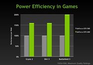
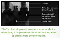
"The advancement that TSMC offered was a new optimized process technology. Kepler is manufactured using TSMC's 28nm high performance (HP) process, the foundry's most advanced 28nm process which uses their first-generation high-K metal gate (HKMG) technology and second generation SiGe (Silicon Germanium) straining," read the blog post. "Using TSMC's 28nm HP process enabled us to reduce active power by about 15 percent and leakage by about 50 percent compared to 40nm, resulting in an overall improvement in power efficiency of about 35 percent (see charts)."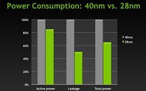
 Apart from advanced process technologies, NVIDIA credited professional collaboration with its long time foundry partner. According to Greco, groundwork for what led to today's Kepler chip began three years before tape-out, over the course of which the two companies set up a "Production Qualification Vehicle (PQV)" that allowed engineers from both sides to optimize the process. "Through repeated prototyping, we were able to optimize both the process and design, creating a more efficient Kepler design rather than simply a chip in a standard 28nm process," he writes. The entire blog post can be read here.
"The advancement that TSMC offered was a new optimized process technology. Kepler is manufactured using TSMC's 28nm high performance (HP) process, the foundry's most advanced 28nm process which uses their first-generation high-K metal gate (HKMG) technology and second generation SiGe (Silicon Germanium) straining," read the blog post. "Using TSMC's 28nm HP process enabled us to reduce active power by about 15 percent and leakage by about 50 percent compared to 40nm, resulting in an overall improvement in power efficiency of about 35 percent (see charts)."


14 Comments on NVIDIA Credits Close Collaboration with TSMC for Kepler's Energy Efficiency
on topic, I have always wondered if power leakage improves as the process(in this case 28nm) matures.. in which case 2nd iteration of kepler will have better perf/watt
...It was published that they (NVDA) didn't do a great job working out the production kinks with TSMC when they slapped Fermi together.
Anyway, good for them, and good for us!
If the process matures enough to squeeze more power out of the chip, it seems like NV's strategy is to tweak the design and release a new model line. Otherwise the differences seem to be minor.
My 580 was better
My current 7970 is a ice machine in comparison to the Nvidia´s....
Is AMD using TSMC or Global Foundries?
and a 7970 vs 680 power draw is about the same, meaning they both generate the same amount of heat in a closed area.
The stock 7970 just has a more aggressive fan profile then a 680 so it's cooler under load but generates more noise.
Except the 7970 doesn't performs as well as a 680 so if anything you're producing unnecessary heat when compared to nvidia, that whole performance per watt crap which is really only valid when discussing efficiency rather irrelevant if you're just talking about performance, top dog is top dog.
They produce around the same amount of heat is what i'm getting at for the most part.
also amd's dedicated gpus are produce at TSMC GF is not nearly up to snuff for that work.
AAAAaaaaa its a BOY!!!! Look at the little pecker :toast:
NVIDIA needs to get on TSMC ass and get some kick ass cheaper mid range cards out ASAP.