Thursday, May 17th 2012

GK110 Packs 2880 CUDA Cores, 384-bit Memory Interface: Die-Shot

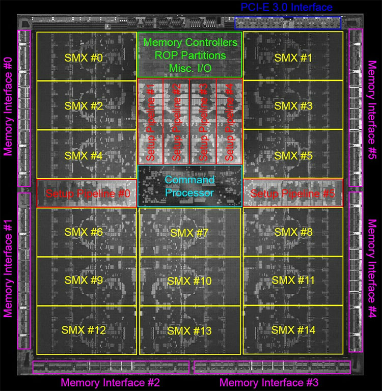
With its competition checked thanks to good performance by its GK104 silicon, NVIDIA was bold enough to release die-shots of its GK110 silicon, which made its market entry as the Tesla K20 GPU-compute accelerator. This opened flood-gates of speculation surrounding minute details of the new chip, from various sources. We found one of these most plausible, by Beyond3D community member "fellix". The source of the image appears to have charted out component layout of the chip by some pattern recognition and educated guesswork.

It identifies the the 7.1 billion transistor GK110 silicon to have 15 streaming multiprocessors (SMX). A little earlier this week, sources close to NVIDIA confirmed the SMX count to TechPowerUp. NVIDIA revealed that the chip will retain the SMX design of GK104, in which each of these holds 192 CUDA cores. Going by that, GK110 has a total of 2880 cores. Blocks of SMX units surround a centrally-located command processor, along with six setup pipelines, and a portion holding the ROPs and memory controllers. There are a total of six GDDR5 PHYs, which could amount to a 384-bit wide memory interface. The chip talks to the rest of the system over PCI-Express 3.0.
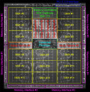
Source: Beyond3D Forum
Add your own comment

65 Comments on GK110 Packs 2880 CUDA Cores, 384-bit Memory Interface: Die-Shot

#51
Disparia
qubit...

Thing is, I did actually learn the basics of designing integrated digital circuits at uni many moons ago and they tought me that building them out to the full power of 2 always maximises the design and they explained exactly why. This principle remains true regardless of what process technology is used or how fancy and complicated the design is.

...

It's hard for me to explain why in words here the exact reasons why building an IC out to the power of 2 is optimal (and perhaps someone else can do it better) which is why I advised erocker to consider the small, low end graphics cards as an explanation because for those, the physical budget is there to build them out to the full power of 2.
Hope you still have some notes from class? ;)

Otherwise I'm not seeing the shame in it. Before Fermi memory addressing was 32bit (storing 64bit values in multiple 32bit address - now that is far from optimal!). With 64bit addressing in Fermi and newer, seems like each access would occur on 1 (possibly 2?) of it's 6 memory controllers. There's not enough nitty gritty information in the GK110 whitepaper nor understanding on my part to say anything definitive about how their memory management works.

And in reality, suboptimal or not, I'll take 384bit over 320bit over 256bit. If they want to give me 448bit or 512bit, that would awesome too. Well, awesome in theory. I still haven't been able to work up the case for the company to buy Teslas for my servers :D
Posted on Reply
#52
ypsylon
Really funny reading some answers (over many, many forums). Boys and girls you haven't got a clue how much Tesla cards cost and at what segment are aimed.

Ask yourself: WTH would buy industrial VGA for home use with price at 4000+ USD/Euro? Nobody cares about games with Teslas. Don't compare GeForce with Tesla or Quadro. Like comparing old rusty bike to Ferrari or SLR Mercedes.
Posted on Reply
#53
Steevo
ypsylonReally funny reading some answers (over many, many forums). Boys and girls you haven't got a clue how much Tesla cards cost and at what segment are aimed.

Ask yourself: WTH would buy industrial VGA for home use with price at 4000+ USD/Euro? Nobody cares about games with Teslas. Don't compare GeForce with Tesla or Quadro. Like comparing old rusty bike to Ferrari or SLR Mercedes.
Thanks gramps.....all of us boys and girls who don't work and live in our parents basements and dream of making $5 a hour know nothing. We sure are glad we can jump on our rusty old bike and go play with our friends after we game on our mom's old Inspiron with a 6400 graphics card and shoot them up real good and fast with our Intel Gigahurts processor.

Maybe you could come over and show us your fancy car and stuff, and bring us icecream and other treats huh?
Posted on Reply
#54
qubit
Overclocked quantum bit
SteevoThanks gramps.....all of us boys and girls who don't work and live in our parents basements and dream of making $5 a hour know nothing. We sure are glad we can jump on our rusty old bike and go play with our friends after we game on our mom's old Inspiron with a 6400 graphics card and shoot them up real good and fast with our Intel Gigahurts processor.

Maybe you could come over and show us your fancy car and stuff, and bring us icecream and other treats huh?
:roll:
Posted on Reply
#55
Sinzia
SteevoThanks gramps.....all of us boys and girls who don't work and live in our parents basements and dream of making $5 a hour know nothing. We sure are glad we can jump on our rusty old bike and go play with our friends after we game on our mom's old Inspiron with a 6400 graphics card and shoot them up real good and fast with our Intel Gigahurts processor.

Maybe you could come over and show us your fancy car and stuff, and bring us icecream and other treats huh?
Had to laugh at this one, thanks.

I'm doubtful we'll see a GK110 based gaming card this generation, seems GK110 will be the compute (read: Tesla) card.
Posted on Reply
#56
TheoneandonlyMrK
SinziaI'm doubtful we'll see a GK110 based gaming card this generation, seems GK110 will be the compute (read: Tesla) card.
i dont see how you get to that result , if they are makeing GK110 then they are producing across bins ,this spec of part might not Be the highest but probably is, either way their Will be less capable chips, they'r not literall bins, the poorer cousins ,lets just call em will see light of day too , i dont see a scenario where they can Not do some kind of consumer card due to the lower binned parts normally outnumbering full spec chips

i would say this spec of GK110 chip wont hit consumer cards until the 7xx imho
Posted on Reply
#57
radrok
SinziaHad to laugh at this one, thanks.

I'm doubtful we'll see a GK110 based gaming card this generation, seems GK110 will be the compute (read: Tesla) card.
I'm more inclined to think like Sinzia, such a big chip would probably be hard to use in consumer products with noticeable profits, this is ever bigger than GF100/110, if I'm not mistaken.

Anyway I think it all depends on AMD/ATI 89xx series and how early they will launch it.
Nvidia may just continue using smaller chips on their Geforce lineup because they are less likely to encounter yield issues and huge costs linked to very big chip designs.
Posted on Reply
#58
Steevo
radrokI'm more inclined to think like Sinzia, such a big chip would probably be hard to use in consumer products with noticeable profits, this is ever bigger than GF100/110, if I'm not mistaken.

Anyway I think it all depends on AMD/ATI 89xx series and how early they will launch it.
Nvidia may just continue using smaller chips on their Geforce lineup because they are less likely to encounter yield issues and huge costs linked to very big chip designs.
They seemingly learned from Fermi and the schlacking they took on it. You make significantly less is you have more die area, and that is what they are selling, a GPU die. Plus every extra mm means the dies have a higher chance of flaws, more power gates are needed or more core voltage to maintain stability at a set speed. It just makes sense to make it more efficient and achieve a higher frequency than to aim for bigger dies. The 670 is a prime example of this. That is an amazing card.
Posted on Reply
#59
EpicShweetness
www.nvidia.com/content/PDF/kepler/NVIDIA-Kepler-GK110-Architecture-Whitepaper.pdf

This PDF will help with the speculation's and such. Apparently there are 16 Texture Units per SMX 240 total! The L2 Cache is double so one can only speculate double the ROP's (128). The core clock and memory clock is still unknown, but the data compiling on this monstrosity is staggering! I would gladly pay $600 or $700 on a chip of this magnitude, well if I needed that much power my 7870 is amazing all by it's self.
Posted on Reply
#60
largon
According to the looks of GK110 die shot amount of ROPs is the same as Fermi's.
Posted on Reply
#61
Johannesburg
hardcore_gamerNvidia should fix the yield issues and make 680s available before making SKUs with even bigger die.
Maybe TSMC should fix their problems for themselves. ;)
Posted on Reply
#62
Xzibit
JohannesburgMaybe TSMC should fix their problems for themselves. ;)
I dont think TSMC has a problem. They provide a service which is indemand. Its a have your own means or rely on someone else.

Few companies take the time and money to invest to be self reliant if your not you get in line along with the rest of them.
Posted on Reply
#63
Xzibit
Since I havent seen any updated news.

Nvidia Investors meeting was today

The Tesla will be available in Q4 2012. No mention of the GeForce line.
Posted on Reply
#64
Prima.Vera
ypsylonReally funny reading some answers (over many, many forums). Boys and girls you haven't got a clue how much Tesla cards cost and at what segment are aimed.

Ask yourself: WTH would buy industrial VGA for home use with price at 4000+ USD/Euro? Nobody cares about games with Teslas. Don't compare GeForce with Tesla or Quadro. Like comparing old rusty bike to Ferrari or SLR Mercedes.
A better comparison will be between a truck and a Dodge Viper. Both have 8 liter engines but only one can go 300Km/h while the other carry several dozen tones of cargo ;)
Posted on Reply
#65
techtard
And one looks better than the other when you add a lift kit.
Posted on Reply
Add your own comment
Apr 19th, 2024 18:38 EDT change timezone

New Forum Posts

Popular Reviews

Controversial News Posts