Thursday, May 17th 2012

GK110 Packs 2880 CUDA Cores, 384-bit Memory Interface: Die-Shot
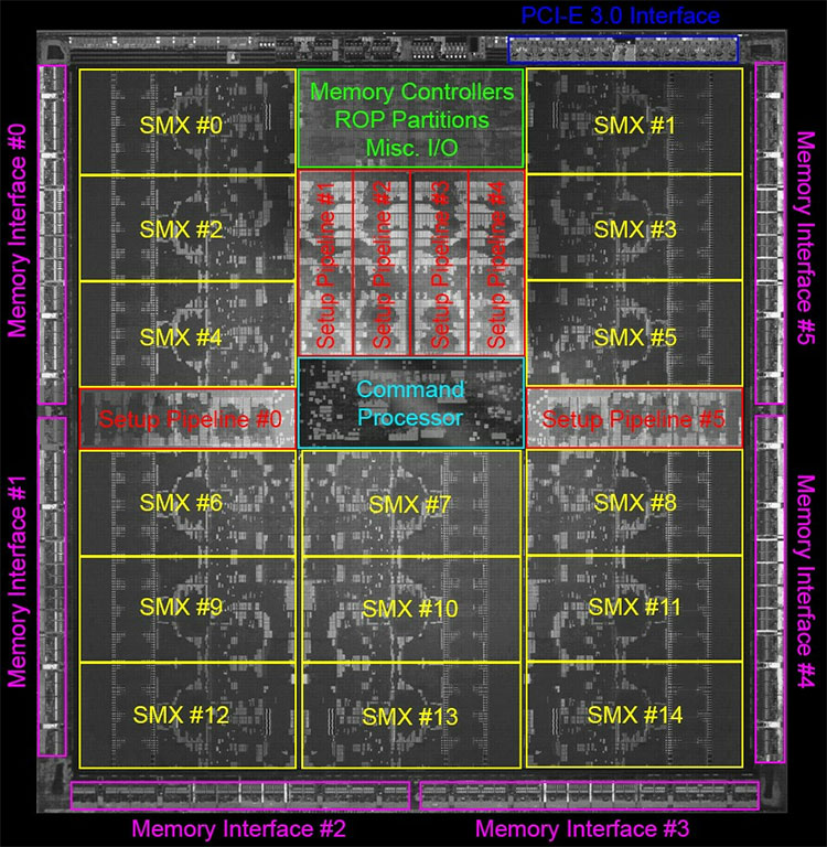
With its competition checked thanks to good performance by its GK104 silicon, NVIDIA was bold enough to release die-shots of its GK110 silicon, which made its market entry as the Tesla K20 GPU-compute accelerator. This opened flood-gates of speculation surrounding minute details of the new chip, from various sources. We found one of these most plausible, by Beyond3D community member "fellix". The source of the image appears to have charted out component layout of the chip by some pattern recognition and educated guesswork.
It identifies the the 7.1 billion transistor GK110 silicon to have 15 streaming multiprocessors (SMX). A little earlier this week, sources close to NVIDIA confirmed the SMX count to TechPowerUp. NVIDIA revealed that the chip will retain the SMX design of GK104, in which each of these holds 192 CUDA cores. Going by that, GK110 has a total of 2880 cores. Blocks of SMX units surround a centrally-located command processor, along with six setup pipelines, and a portion holding the ROPs and memory controllers. There are a total of six GDDR5 PHYs, which could amount to a 384-bit wide memory interface. The chip talks to the rest of the system over PCI-Express 3.0.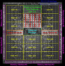
Source:
Beyond3D Forum
It identifies the the 7.1 billion transistor GK110 silicon to have 15 streaming multiprocessors (SMX). A little earlier this week, sources close to NVIDIA confirmed the SMX count to TechPowerUp. NVIDIA revealed that the chip will retain the SMX design of GK104, in which each of these holds 192 CUDA cores. Going by that, GK110 has a total of 2880 cores. Blocks of SMX units surround a centrally-located command processor, along with six setup pipelines, and a portion holding the ROPs and memory controllers. There are a total of six GDDR5 PHYs, which could amount to a 384-bit wide memory interface. The chip talks to the rest of the system over PCI-Express 3.0.
65 Comments on GK110 Packs 2880 CUDA Cores, 384-bit Memory Interface: Die-Shot
I've read almost everything available about them, and GCN and previous AMD/Ati chips. So be clear about what you mean because you make zero sense.
*Optimized is when the design of a base 2 (binary) digital circuit fills out the binary address range ie a power of 2. All the components within the chip should follow the power of 2 to do it properly, of course. For example, that would mean using 16 SMX units with 256 CUDA cores each, etc.
More expensive
512 bit bus really isn't necessary at all, especially with QDR memory.
That being said, I want this card. Hopefully it comes as the 7 series and is priced right.
I wish I could show you what the difference would be, but I have no practical way of demonstrating it. I guess one way to look at it is to check out the really low end cards, as they're quite often optimized in this way, because they don't take a huge transistor budget and not a lot of heat and power, either, so they can afford to do this in a physical product.
I do Autocad, bring on the cores I say..
I definitely desire this card, but will most likely never own it :laugh: GTX570 can keep me going until the next gen consoles raise the bar I think
and i think it telling that their K10 has two gpu's a clear cost disavantage(in manufacture) when all prior gens started with single gpu compute cards, this chip is simply worse then the last for this purpose, they threw amd and intel a bone in this dept imho.
Release the kraken already!!.....err, i mean release the god damned GTX 660 Ti variant...
$200 and below :D
@Benetanegia: i thought the superb performance per watt of gk104 was because they crippled its compute performance?I would prefer to spend my hard earned money on a GTX680 or a 1150Mhz saphire 7970, you know, all the prettyness in the world (GTX 690), won't save it from microstutter.
I'm surprised you actually thanked him for that useless post, erocker.
Maybe wait until there is solid evidence of when Nvidia will even bother to turn this thing into a GeForce variant and how it will castrate it.
Obviously it wasnt possible hence they made GK104 and J H-H said if it was feasable to do he would do it but as it is now its not as he mention to investors.
I very much doubt he meant it in a serious way
Thing is, I did actually learn the basics of designing integrated digital circuits at uni many moons ago and they tought me that building them out to the full power of 2 always maximises the design and they explained exactly why. This principle remains true regardless of what process technology is used or how fancy and complicated the design is.
Unfortunately, the chip literally grows exponentially in size as you do this and the semiconductor companies like nvidia, amd and Intel know this all too well, so in a real-world device, one is always limited by things such as transistor budget, physical size, reducing clock speed (fan-out/fan-in) limitations) power and heat etc. Hence, you get these odd, lopsided designs. The 384-bit bus is just one manifestation of this necessary compromise. It's just a shame to see it, which was my point in my original post on this thread.
It's hard for me to explain why in words here the exact reasons why building an IC out to the power of 2 is optimal (and perhaps someone else can do it better) which is why I advised erocker to consider the small, low end graphics cards as an explanation because for those, the physical budget is there to build them out to the full power of 2.
But a overclocked 670 with 192 less cuda cores and 4% faster base clock rate is only 1% faster than a stock 680.
Do the math, frequency counts more with this than cluster counts, they went the way they did to attain such great clocks to meet their performance needs. I see this being 70% of the speed of a 690, it just needs to be priced accordingly.
could the additional 128bits of nvidias bus not be iommu too, given they are adearing to the same pciex3 spec and afaik it calls for virtualized memory support, something they both claim as doable in this gen ,and nvidia anounced VGX which surely needs iommu support??.
Will it be faster at compute tasks? Absolutely. Much in the same way ATI used to have multiple shaders though it will be harder to schedule for, much like what ATI had to use drivers to do setup on for years. I think it will be interesting to see what performance is with different CPU's.