Monday, February 18th 2013

NVIDIA GeForce GTX Titan Graphics Card Pictured in Full

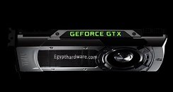
Here it is, folks; the first pictures of NVIDIA's newest pixel crunching dreadnought, the GeForce GTX Titan. Pictures leaked by various sources east of the Greenwich Median reveal a reference board design that's similar in many ways to that of the GeForce GTX 690, thanks to the magnesium alloy cooler shroud, a clear acrylic window letting you peep into the aluminum fin stack, and a large lateral blower. The card features a glowy "GeForce GTX" logo much like the GTX 690, draws power from a combination of 6-pin and 8-pin PCIe power connectors, and features two SLI bridge fingers letting you pair four of them to run 3DMark Fire Strike as if it were a console port from last decade.
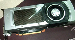
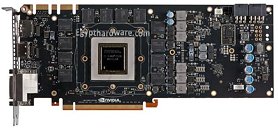
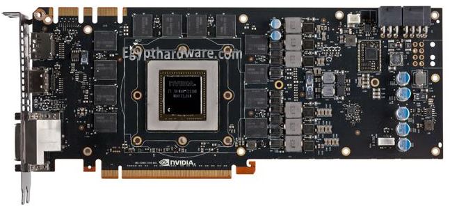
The GeForce GTX Titan PCB reveals that NVIDIA isn't using a full-coverage IHS on the GK110 ASIC, rather just a support brace. This allows enthusiasts to apply TIM directly on the chip's die. The GPU is wired to a total of twenty four 2 Gbit GDDR5 memory chips, twelve on each side of the PCB. The card's VRM appears to consist of a 6+2 phase design which uses tantalum capacitors, slimline chokes, and driver-MOSFETs. The PCB features a 4-pin PWM fan power output, and a 2-pin LED logo power output that's software controllable.

Given the rumored specifications of the GTX Titan, the card could be overkill for even 2560 x 1600, and as such could be designed for 3DVision Surround (3 display) setups. Display outputs include two dual-link DVI, an HDMI, and a DisplayPort.

According to most sources, the card's specifications look something like this:
  • 28 nm GK110-based ASIC
  • 2,688 CUDA cores ("Kepler" micro-architecture)
  • 224 TMUs, 48 ROPs
  • 384-bit GDDR5 memory interface
  • 6 GB memory
  • Clocks:
    o 837 MHz core
    o 878 MHz maximum GPU Boost
    o 6008 MHz memory
  • 250W board power
Sources: Egypt Hardware, VideoCardz
Add your own comment

118 Comments on NVIDIA GeForce GTX Titan Graphics Card Pictured in Full

#101
xenocide
jihadjoeDont forget how Nvidia dropped the 8800GT, offering 90% of the performance of the super-pricey 8800GTX while costing less than half as much.
Or the fact that the top end of Nvidia's GPUs has been on the decline since then;

Nvidia Launch Prices:
GTX280 - $650
GTX480 - $500
GTX580 - $500
GTX680 - $499

Granted not a huge drop towards the end, but I think $500 for the pinnacle of GPU performance is somewhat a sweet spot.
Crowned ClownAre they going to cripple it again so it'll become useless for 3ds max design gpu accelerated rendering? so that I'll be forced to buy their super uber premium stupendously expensive quadro 6000 video card. :confused:

My 680 cant even use quicksilver and mental ray; its slow in opengl apps like google sketchup as well. I wonder if this one to is.
Nope. The GK110 should be a revision of the GK100, which was the successor to the GTX580. That means all that compute functionality that was stripped away from GTX680 is back and presumably better than ever.
BigMack70It's always kinda dumb to compare an overclocked card to a stock one. The Titan card will overclock at least somewhat, and only then can you compare a manually overclocked 7970 to a (manually OC'd) Titan. While I agree that what Nvidia is bringing to the table isn't particularly impressive (according to the info we have now), the reason has more to do with price than anything else.

Not many 7970s, even Matrix ones, will hit 1300 MHz on air.
If I recall, didn't the HD7970 launch with clocks similar to what is reported for Titan? Around 800-850 MHz? Who's to say the Titan won't overclock at least as well? GK104 and Tahiti have had no problems being stretched upwards of 30% for retail cards...
Posted on Reply
#102
Cuzza
Dude, you can't pair four of something. A pair is two.
Posted on Reply
#103
BigMack70
xenocideIf I recall, didn't the HD7970 launch with clocks similar to what is reported for Titan? Around 800-850 MHz? Who's to say the Titan won't overclock at least as well? GK104 and Tahiti have had no problems being stretched upwards of 30% for retail cards...
The 7970 launched at 925 MHz and the average overclock is around 1200 Mhz, which is crazy.

Average % OCs are a bit less for GTX 670/680 in comparison.

I am curious to see how this Titan card OCs. I'm glad they're supposedly restoring real voltage control to the card, but with the chip being so large (7.1B transistors!!!), I kind of doubt that it's going to OC much more than 10-15%.

The big average overclocks seen from the 7950 and 7970 are somewhat uncommon for high end GPUs.
Posted on Reply
#104
NeoXF
OK, I'm done in this thread. Had enough of fanboys or people with pockets deeper then their intellect/sanity well for one day. Enjoy your crummy stillborn stopgap GPU.

And for the record, when I saw ocholic.ch's "review" of it, I was absolutely ecstatic about getting one during the summer maybe... even tho they smelled like complete bullshit... Thanks nVidia for confirming that... no GPUs to look forward to anytime soon then...
Posted on Reply
#105
xorbe
~850MHz? What'll it do under water @ 1150 and 400 watts ...
Posted on Reply
#106
tastegw
NeoXFOK, I'm done in this thread. Had enough of fanboys or people with pockets deeper then their intellect/sanity well for one day. Enjoy your crummy stillborn stopgap GPU.

And for the record, when I saw ocholic.ch's "review" of it, I was absolutely ecstatic about getting one during the summer maybe... even tho they smelled like complete bullshit... Thanks nVidia for confirming that... no GPUs to look forward to anytime soon then...
Posted on Reply
#107
eidairaman1
The Exiled Airman
Crowned ClownAre they going to cripple it again so it'll become useless for 3ds max design gpu accelerated rendering? so that I'll be forced to buy their super uber premium stupendously expensive quadro 6000 video card. :confused:

My 680 cant even use quicksilver and mental ray; its slow in opengl apps like google sketchup as well. I wonder if this one to is.
for professional graphics its all how the driver is setup a desktop driver is not the same as a professional driver, at least back in the day some GF and Radeon Cards could be converted over to the Quadro and Fire GL Series via a bios flash and use of the proper drivers for those cards
Posted on Reply
#108
valentyn0
NeoXFOK, I'm done in this thread. Had enough of fanboys or people with pockets deeper then their intellect/sanity well for one day. Enjoy your crummy stillborn stopgap GPU.

And for the record, when I saw ocholic.ch's "review" of it, I was absolutely ecstatic about getting one during the summer maybe... even tho they smelled like complete bullshit... Thanks nVidia for confirming that... no GPUs to look forward to anytime soon then...
That's ironic, considering i was about to say earlier, to chill down, amd fanboy!
Posted on Reply
#110
Crowned Clown
xenocideNope. The GK110 should be a revision of the GK100, which was the successor to the GTX580. That means all that compute functionality that was stripped away from GTX680 is back and presumably better than ever.
need some reviews before I'd jump to a 1K price tagged gpu. I wanna see how it performs in 3d rendering.
eidairaman1for professional graphics its all how the driver is setup a desktop driver is not the same as a professional driver, at least back in the day some GF and Radeon Cards could be converted over to the Quadro and Fire GL Series via a bios flash and use of the proper drivers for those cards
Never knew that, so I did some experiment and bought a low prof pro gpu; a $130 quaddro 410 that performs 10x better in sketchup than my 680. :laugh:
Posted on Reply
#111
brandonwh64
Addicted to Bacon and StarCrunches!!!
Fan boi this fan boi that. I love these threads.
Posted on Reply
#112
Horrux
eidairaman1for professional graphics its all how the driver is setup a desktop driver is not the same as a professional driver, at least back in the day some GF and Radeon Cards could be converted over to the Quadro and Fire GL Series via a bios flash and use of the proper drivers for those cards
I thought it had more to do with the silicon's error testing process, which (I thought) was long and involved for professional workstation GPUs and rudimentary for gaming GPUs. The logic being that you really need error free graphics computation in the pro market but not for gaming.

Actually, I'm fairly certain this is still the case. Converting a gaming GPU to a "workstation" GPU through a bios flash will make a gaming GPU appear to be a workstation GPU, but it doesn't mean it will have the same lack of computation error...
Posted on Reply
#113
Xzibit
CuzzaDude, you can't pair four of something. A pair is two.
I beg to differ.

Boobs :)

If I have 1 girl I get 2 or X-Fire/SLI.
If I have a pair of girls I have 4 or Quad-Fire/Quad-SLI
Posted on Reply
#114
eidairaman1
The Exiled Airman
HorruxI thought it had more to do with the silicon's error testing process, which (I thought) was long and involved for professional workstation GPUs and rudimentary for gaming GPUs. The logic being that you really need error free graphics computation in the pro market but not for gaming.

Actually, I'm fairly certain this is still the case. Converting a gaming GPU to a "workstation" GPU through a bios flash will make a gaming GPU appear to be a workstation GPU, but it doesn't mean it will have the same lack of computation error...
you ever compared specs between certain cards, they are exactly the same, on the professional side its all about those drivers and software
Posted on Reply
#115
johnspack
Here For Good!
I want four of these, and 2 of them I'll break up and smoke for 3 months straight.....
Posted on Reply
#116
HumanSmoke
eidairaman1you ever compared specs between certain cards, they are exactly the same, on the professional side its all about those drivers and software
Not entirely. Both you and Horrux are correct.
Pro cards like the Tesla have a much more rigorous validation procedure which goes far beyond crafting UMD's (User Mode Drivers) and in-place ongoing test evaluation, so while the GPUs are binned for voltage and usable logic blocks, you'd find that a more fine scaled binning is also being used to test the integrity of the logic blocks that are functional. I don't think the binning of pro GPUs differs a great deal from pro CPUs like Xeon and Opteron in that respect.
Posted on Reply
#117
Horrux
eidairaman1you ever compared specs between certain cards, they are exactly the same, on the professional side its all about those drivers and software
I know my shiz bro. I come across as humble, because I am, but I still know tech. ;)
Posted on Reply
#118
eidairaman1
The Exiled Airman
HumanSmokeNot entirely. Both you and Horrux are correct.
Pro cards like the Tesla have a much more rigorous validation procedure which goes far beyond crafting UMD's (User Mode Drivers) and in-place ongoing test evaluation, so while the GPUs are binned for voltage and usable logic blocks, you'd find that a more fine scaled binning is also being used to test the integrity of the logic blocks that are functional. I don't think the binning of pro GPUs differs a great deal from pro CPUs like Xeon and Opteron in that respect.
ya I wouldn't doubt it. I did research on the 5870 and its firegl/firestream counterpart only thing changed was capacity.of ram and clock speeds
HorruxI know my shiz bro. I come across as humble, because I am, but I still know tech. ;)
ok cool dude
Posted on Reply
Add your own comment
Apr 24th, 2024 18:45 EDT change timezone

New Forum Posts

Popular Reviews

Controversial News Posts