Monday, May 5th 2014

GeForce GTX 880 ES Intercepted En Route Testing Lab, Features 8 GB Memory?

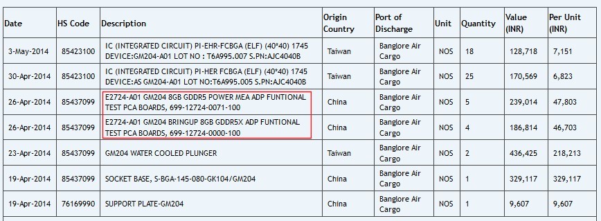
An engineering sample (ES) of the GeForce GTX 880 was intercepted on its way from a factory in China, to NVIDIA's development center in India, where it will probably undergo testing and further development. The shipping manifest of the courier ferrying NVIDIA's precious package was sniffed out by the Chinese press. NVIDIA was rather descriptive about the ES, in its shipping declaration. Buzzwords include "GM204" and "8 GB GDDR5," hinting at what could two of the most important items on its specs sheet. GM204 is a successor of GK104, and is rumored to feature 3,200 CUDA cores, among other things, including a 256-bit wide memory bus. If NVIDIA is cramming 8 GB onto the card, it must be using some very high density memory chips. The manifest also declares its market value at around 47,000 Indian Rupees. It may convert to US $780, but adding all taxes and local markups, 47,000 INR is usually where $500-ish graphics cards end up in the Indian market. The R9 290X, for example, is going for that much.
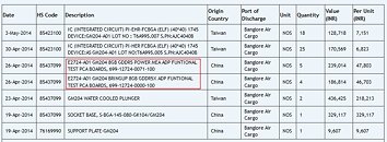
Sources: ChipHell, VideoCardz
Add your own comment

66 Comments on GeForce GTX 880 ES Intercepted En Route Testing Lab, Features 8 GB Memory?

#51
Relayer
cadavecaJust because it makes sense, doesn't make it right, though. Listed memory and shader counts don't make sense to me, and to me point to that dual-GPU... W1zz is probably bang-on as to why there might be an 8 GB listing, however. I hadn't considered that it might have to do with memory controller testing, and that makes even more sense to me. 3000 shaders tops 780 TI though.
I didn't say I'd bet the house on it.
Posted on Reply
#52
cadaveca
My name is Dave
RelayerI didn't say I'd bet the house on it.
Heh. I feel ya. The shader numbers given are still weird, so whateva.
Posted on Reply
#53
EarthDog
NationsAnarchy256-bit memory interface only ? Can someone convince me why not 512 ?
Sure... what is the bandwidth of a 512bit bus running at 1250Mhz versus a 256bit bus running at 1750 Mhz?
(Answer: in the same ballpark)

It is, for the most part, two different ways of getting to the same thing. making a 512bit bus is more expensive, but using 1250Mhz rated DDR5 is cheaper. Versus a cheaper to make bus and more expensive ram IC's.
Posted on Reply
#54
NationsAnarchy
EarthDogSure... what is the bandwidth of a 512bit bus running at 1250Mhz versus a 256bit bus running at 1750 Mhz?
(Answer: in the same ballpark)

It is, for the most part, two different ways of getting to the same thing. making a 512bit bus is more expensive, but using 1250Mhz rated DDR5 is cheaper. Versus a cheaper to make bus and more expensive ram IC's.
I'm down with this one. Thanks man ! I hope I can learn more from you
Posted on Reply
#55
3dhotshot
Nvidia knows a 512 bit memory bus will destroy any and all games at ultra settings even with just a 2GB Gfx card ~ this is just the reason they will only keep the 512bit bus for their flagship products.

512 bit = more heat, this is why I think 8 Gigs of 256 bit ram is the route they are going with.

8GB gddr5 on a graphics card has been long overdue, and these cards will equip the gamer for 3k and 4k gaming. Lets not forget custom GPU resolution scaling on existing drivers allow you to play on resolutions much higher than your current monitor supports. Other people like 3d artists who use software like Lumion / Lightwave 3d / Unreal Engine 4 / Adobe CS suite etc will benefit greatly from these 8gig cards !!!

I vote for 8gigs of ram anytime. They are preparing for smooth fps on next generation game engines.
NationsAnarchy256-bit memory interface only ? Can someone convince me why not 512 ?
Yes I also vote for a 512bit memory bus 8gig Gfx card which is affordable, however Nvidia may not be willing to come to the table instead.... they continue to drag the market and gamers along with it.

Nvidia knows a 512 bit memory bus will destroy any and all games at ultra settings even with just a 2GB Gfx card ~ this is just the reason they will only keep the 512bit bus for their flagship products.

512 bit = more heat, this is why I think 8 Gigs of 256 bit ram is the route they are going with.

8GB gddr5 on a graphics card has been long overdue, and these cards will equip the gamer for 3k and 4k gaming. Lets not forget custom GPU resolution scaling on existing drivers allow you to play on resolutions much higher than your current monitor supports. Other people like 3d artists who use software like Lumion / Lightwave 3d / Unreal Engine 4 / Adobe CS suite etc will benefit greatly from these 8gig cards !!!

I vote for 8gigs of ram anytime. They are preparing for smooth fps on next generation game engines.
Posted on Reply
#56
HumanSmoke
3dhotshotNvidia knows a 512 bit memory bus will destroy any and all games at ultra settings even with just a 2GB Gfx card ~ this is just the reason they will only keep the 512bit bus for their flagship products.
No, it's because memory controllers add die complexity and size. The memory bus also needs to balance the core components. It is why you don't see a 512-bit (or 384 for that matter) used in ANY GPU except the largest die of an architecture.
Care to name ANY GPU regardless of vendor that wasn't a flagship of the architecture that had a high bus width?
3dhotshot512 bit = more heat.
No. Transistor density is actually lower in the uncore ( memory controllers, cache, I/O etc ) than in the core. The only reason that high bus width GPUs use more power is because they are large pieces of silicon with more cores than the mainstream/entry level GPUs.
Posted on Reply
#57
GhostRyder
3dhotshotYes I also vote for a 512bit memory bus 8gig Gfx card which is affordable, however Nvidia may not be willing to come to the table instead.... they continue to drag the market and gamers along with it.

Nvidia knows a 512 bit memory bus will destroy any and all games at ultra settings even with just a 2GB Gfx card ~ this is just the reason they will only keep the 512bit bus for their flagship products.

512 bit = more heat, this is why I think 8 Gigs of 256 bit ram is the route they are going with.

8GB gddr5 on a graphics card has been long overdue, and these cards will equip the gamer for 3k and 4k gaming. Lets not forget custom GPU resolution scaling on existing drivers allow you to play on resolutions much higher than your current monitor supports. Other people like 3d artists who use software like Lumion / Lightwave 3d / Unreal Engine 4 / Adobe CS suite etc will benefit greatly from these 8gig cards !!!

I vote for 8gigs of ram anytime. They are preparing for smooth fps on next generation game engines.
You can make up for the bus being smaller with core clocks which maybe what NVidia is going for here since that's how they have done it before in fact both do something like that as a trade every now and then (AMD and Nvidia). Plus these are only rumors and rumors do change with time. The 8gb itself is what will be king if this turns into the real GTX 880 because that's where Nvidia has been falling behind is with enough ram to run ultra HD setups, 3gb was not cutting it this round.
HumanSmokeNo, it's because memory controllers add die complexity and size. The memory bus also needs to balance the core components. It is why you don't see a 512-bit (or 384 for that matter) used in ANY GPU except the largest die of an architecture.
Care to name ANY GPU regardless of vendor that wasn't a flagship of the architecture that had a high bus width?
Pfft, ok. Try the HD 6850-6870, both had a 256bit bus just like the HD 6950 and 6970. LINK1, link2, link3.
Posted on Reply
#58
xenocide
GhostRyderThe 8gb itself is what will be king if this turns into the real GTX 880 because that's where Nvidia has been falling behind is with enough ram to run ultra HD setups, 3gb was not cutting it this round.
Except that it was. Ultra HD is defined as 4K+, do you seriously think any current GPU will run out of VRAM before it runs out of processing power at that high of a resolution?
GhostRyderPfft, ok. Try the HD 6850-6870, both had a 256bit bus just like the HD 6950 and 6970. LINK1, link2, link3.
HD6850 and HD6870 were basically revised versions of HD5850 and HD5870--AMD's former flagship. Plus, AMD switched from VLIW5 to VLIW4 between Barts and Cayman.
Posted on Reply
#59
GhostRyder
xenocideHD6850 and HD6870 were basically revised versions of HD5850 and HD5870--AMD's former flagship. Plus, AMD switched from VLIW5 to VLIW4 between Barts and Cayman.
But Barts was not the flagship of that generation, Cayman was and they still had a 256bit bus just like it.
xenocideExcept that it was. Ultra HD is defined as 4K+, do you seriously think any current GPU will run out of VRAM before it runs out of processing power at that high of a resolution?
At 4k is what I was referring to, that resolution has already seen the 3gb maxing out and causes the gap that the GTX 780ti had gotten over the 290x to become lower than at the lower resolutions. In Multi-GPU setups, the 290X even takes the lead in many situations or keeps it within a few FPS average difference. The new EVGA GTX 780ti 6gb edition solves that problem out right or this next gen maxwell will.
Posted on Reply
#60
xenocide
GhostRyderBut Barts was not the flagship of that generation, Cayman was and they still had a 256bit bus just like it.
Because it was a repackaged flagship product. Using that same logic a GTX 760 or 770 also somewhat proves the point.
GhostRyderAt 4k is what I was referring to, that resolution has already seen the 3gb maxing out and causes the gap that the GTX 780ti had gotten over the 290x to become lower than at the lower resolutions. In Multi-GPU setups, the 290X even takes the lead in many situations or keeps it within a few FPS average difference. The new EVGA GTX 780ti 6gb edition solves that problem out right or this next gen maxwell will.
Prove it. Show me a single benchmark of the 780Ti with 6GB vastly outperforming the 3GB version. I cannot find a single one. For that matter, find me a good example of a card offering significant performance gains from doubling the VRAM period. Because I can show you dozens of benchmarks saying it makes no difference.
Posted on Reply
#61
GhostRyder
xenocideBecause it was a repackaged flagship product. Using that same logic a GTX 760 or 770 also somewhat proves the point.
Confused by your wording a bit, it was repackaged yes but the highest performing card of that generation was cayman which in the end of the day was still VLIW architecture. Hawaii vs Tahiti could be viewed the same way in the fact they are both GCN yet the revision number still seems to be a confused point where its either considered 1.1 or 2.0 GCN depending on where you look. But at the end of the day, they are still all part of GCN.
xenocideProve it. Show me a single benchmark of the 780Ti with 6GB vastly outperforming the 3GB version. I cannot find a single one. For that matter, find me a good example of a card offering significant performance gains from doubling the VRAM period. Because I can show you dozens of benchmarks saying it makes no difference.
Ok link, very game dependent but you can see the 290X does use beyond 3gb of memory on games like Crysis 3. As far as a 6gb 780, kinda hard to show since they are pretty new to the market still.
Posted on Reply
#62
HumanSmoke
GhostRyder
HumanSmokeNo, it's because memory controllers add die complexity and size. The memory bus also needs to balance the core components. It is why you don't see a 512-bit (or 384 for that matter) used in ANY GPU except the largest die of an architecture.
Care to name ANY GPU regardless of vendor that wasn't a flagship of the architecture that had a high bus width?
Pfft, ok. Try the HD 6850-6870, both had a 256bit bus just like the HD 6950 and 6970. LINK1, link2, link3.
Pfft. Try again. This time take your time reading what's written. I've added a subtle hint to help you.

--------------------------------------------------------------------------------------------------------


BTW, if you consider 256-bit some kind of pinnacle of bus width, then I'm sureGT 230 owners amongst others would be truly surprised.
...and why prattle on about Cayman? Every man and his dog knows that the R970 was bandwidth starved, and was a principle reason why Tahiti added IMC's. From Anand's Tahiti review:
As it turns out, there’s a very good reason that AMD went this route. ROP operations are extremely bandwidth intensive, so much so that even when pairing up ROPs with memory controllers, the ROPs are often still starved of memory bandwidth. With Cayman AMD was not able to reach their peak theoretical ROP throughput even in synthetic tests, never mind in real-world usage.
xenocideExcept that it was. Ultra HD is defined as 4K+, do you seriously think any current GPU will run out of VRAM before it runs out of processing power at that high of a resolution?
Some people on the internet said it is true, so some other people believe it. The main differences between AMD and Nvidia's architecture re: 4K, are raster throughput and its relative ratio to the number of compute units (or SMX's in Nvidia's case), scheduling of instructions, latency, and cache setup.
Raw bandwidth and framebuffer numbers don't take into account the fundamental difference in architectures, which is why a 256-bit GK 104 with 192 Gb/s of bandwidth can basically live in the same performance neighbourhood as a 384-bit Tahiti with 288 Gb/s. within the confines of a narrow gaming focus.
Posted on Reply
#63
GhostRyder
HumanSmokePfft. Try again. This time take your time reading what's written. I've added a subtle hint to help you.

BTW, if you consider 256-bit some kind of pinnacle of bus width, then I'm sureGT 230 owners amongst others would be truly surprised.
...and why prattle on about Cayman? Every man and his dog knows that the R970 was bandwidth starved, and was a principle reason why Tahiti added IMC's. From Anand's Tahiti review:
Pfft, it was the highest of that architecture at that time, your quote said:
HumanSmokeCare to name ANY GPU regardless of vendor that wasn't a flagship of the architecture that had a high bus width?
Its old get over it, you just said that and it was the HIGHEST of the VLIW architecture meaning your wrong. Trying to change it by saying its not that high compared to todays standards does not mean anything because memory when were talking about a card from a couple years ago especially since 256 bit bus width is still being used on many mid range cards these days. The highest at the generational battles from Nvidia was the 384 bit bus on the GTX 580 for a single GPU at that generational POINT.
Posted on Reply
#64
HumanSmoke
GhostRyderPfft, it was the highest of that architecture at that time, your quote said:
HumanSmokeNo, it's because memory controllers add die complexity and size. The memory bus also needs to balance the core components. It is why you don't see a 512-bit (or 384 for that matter) used in ANY GPU except the largest die of an architecture.
Care to name ANY GPU regardless of vendor that wasn't a flagship of the architecture that had a high bus width?
My god, did you fail learning at school. Why prattle on about the HD 6970 when I was speaking of second tier and lower GPUs. My quote you yourself quoted makes that abundantly clear.
:shadedshu: :roll:

You can hone your "refuting points that aren't being put forward" skills with someone else. I see it as lazy, boring, and counterproductive.
Posted on Reply
#65
GhostRyder
HumanSmokeMy god, did you fail learning at school. Why prattle on about the HD 6970 when I was speaking of second tier and lower GPUs. My quote you yourself quoted makes that abundantly clear.
:shadedshu: :roll:

You can hone your "refuting points that aren't being put forward" skills with someone else. I see it as lazy, boring, and counterproductive.
HD 6870 is a second Tier GPU and had a 256 bit bus same as the HD 6970 which was the flagship of that generation. Nice try changing the subject again...
HumanSmokeCare to name ANY GPU regardless of vendor that wasn't a flagship of the architecture that had a high bus width?
GhostRyderTry the HD 6850-6870, both had a 256bit bus just like the HD 6950 and 6970. LINK1, link2, link3.
Apparently reading is not your strong suit.
6870 = 256bit
6970 = 256bit
6870 is not the highest of that generation, 6970 is, that was high back then...The only card that had a higher bus at that generational point was its competitor the GTX 580.
Posted on Reply
#66
xenocide
GhostRyderOk link, very game dependent but you can see the 290X does use beyond 3gb of memory on games like Crysis 3. As far as a 6gb 780, kinda hard to show since they are pretty new to the market still.
There are plenty of games that use more than 3GB of VRAM, it doesn't mean you will see any real performance boost from adding more of it. Case in point; hexus.net/tech/reviews/graphics/43109-evga-geforce-gtx-680-classified-4gb/?page=7 . BF3 can use more than 3GB of VRAM at 5760x1080, and the difference between a 4GB and 2GB GTX 680 is nonexistant (the 4GB version is also clocked a bit higher so take any gains with a grain of salt). Here's exactly what they said about Crysis 2 during their review:
Of more interest is the 2,204MB framebuffer usage when running the EVGA card, suggesting that the game, set to Ultra quality, is stifled by the standard GTX 680's 2GB. We ran the game on both GTX 680s directly after one another and didn't feel the extra smoothness implied by the results of the 4GB-totin' card.
Just to discredit any notion that I'm cherry picking here's Anandtech reaching a similar conclusion. And Guru3D. And oh look, TPU's own review. The only review I found that has results in favor of a 4GB variation of the GTX 680 was LegionHardware testing at 7680x1600, and still only getting like 12fps, in other words, the gpu ran out of power before memory really became a factor.
Posted on Reply
Add your own comment
Apr 23rd, 2024 18:03 EDT change timezone

New Forum Posts

Popular Reviews

Controversial News Posts