Monday, June 5th 2017

IBM Research Alliance Builds New Transistor for 5 nm Technology
IBM, its Research Alliance partners GLOBALFOUNDRIES and Samsung, and equipment suppliers have developed an industry-first process to build silicon nanosheet transistors that will enable 5 nanometer (nm) chips. The details of the process will be presented at the 2017 Symposia on VLSI Technology and Circuits conference in Kyoto, Japan. In less than two years since developing a 7 nm test node chip with 20 billion transistors, scientists have paved the way for 30 billion switches on a fingernail-sized chip.
The resulting increase in performance will help accelerate cognitive computing, the Internet of Things (IoT), and other data-intensive applications delivered in the cloud. The power savings could also mean that the batteries in smartphones and other mobile products could last two to three times longer than today's devices, before needing to be charged.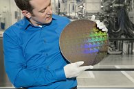 Scientists working as part of the IBM-led Research Alliance at the SUNY Polytechnic Institute Colleges of Nanoscale Science and Engineering's NanoTech Complex in Albany, NY achieved the breakthrough by using stacks of silicon nanosheets as the device structure of the transistor, instead of the standard FinFET architecture, which is the blueprint for the semiconductor industry up through 7 nm node technology.
"For business and society to meet the demands of cognitive and cloud computing in the coming years, advancement in semiconductor technology is essential," said Arvind Krishna, senior vice president, Hybrid Cloud, and director, IBM Research. "That's why IBM aggressively pursues new and different architectures and materials that push the limits of this industry, and brings them to market in technologies like mainframes and our cognitive systems."
The silicon nanosheet transistor demonstration, as detailed in the Research Alliance paper Stacked Nanosheet Gate-All-Around Transistor to Enable Scaling Beyond FinFET, and published by VLSI, proves that 5nm chips are possible, more powerful, and not too far off in the future.
Compared to the leading edge 10nm technology available in the market, a nanosheet-based 5nm technology can deliver 40 percent performance enhancement at fixed power, or 75 percent power savings at matched performance. This improvement enables a significant boost to meeting the future demands of artificial intelligence (AI) systems, virtual reality and mobile devices.
Building a New Switch
"This announcement is the latest example of the world-class research that continues to emerge from our groundbreaking public-private partnership in New York," said Gary Patton, CTO and Head of Worldwide R&D at GLOBALFOUNDRIES. "As we make progress toward commercializing 7nm in 2018 at our Fab 8 manufacturing facility, we are actively pursuing next-generation technologies at 5nm and beyond to maintain technology leadership and enable our customers to produce a smaller, faster, and more cost efficient generation of semiconductors."
IBM Research has explored nanosheet semiconductor technology for more than 10 years. This work is the first in the industry to demonstrate the feasibility to design and fabricate stacked nanosheet devices with electrical properties superior to FinFET architecture.
This same Extreme Ultraviolet (EUV) lithography approach used to produce the 7nm test node and its 20 billion transistors was applied to the nanosheet transistor architecture. Using EUV lithography, the width of the nanosheets can be adjusted continuously, all within a single manufacturing process or chip design. This adjustability permits the fine-tuning of performance and power for specific circuits - something not possible with today's FinFET transistor architecture production, which is limited by its current-carrying fin height. Therefore, while FinFET chips can scale to 5nm, simply reducing the amount of space between fins does not provide increased current flow for additional performance.
"Today's announcement continues the public-private model collaboration with IBM that is energizing SUNY-Polytechnic's, Albany's, and New York State's leadership and innovation in developing next generation technologies," said Dr. Bahgat Sammakia, Interim President, SUNY Polytechnic Institute. "We believe that enabling the first 5nm transistor is a significant milestone for the entire semiconductor industry as we continue to push beyond the limitations of our current capabilities. SUNY Poly's partnership with IBM and Empire State Development is a perfect example of how Industry, Government and Academia can successfully collaborate and have a broad and positive impact on society."
Part of IBM's $3 billion, five-year investment in chip R&D (announced in 2014), the proof of nanosheet architecture scaling to a 5nm node continues IBM's legacy of historic contributions to silicon and semiconductor innovation. They include the invention or first implementation of the single cell DRAM, the Dennard Scaling Laws, chemically amplified photoresists, copper interconnect wiring, Silicon on Insulator, strained engineering, multi core microprocessors, immersion lithography, high speed SiGe, High-k gate dielectrics, embedded DRAM, 3D chip stacking and Air gap insulators.
The resulting increase in performance will help accelerate cognitive computing, the Internet of Things (IoT), and other data-intensive applications delivered in the cloud. The power savings could also mean that the batteries in smartphones and other mobile products could last two to three times longer than today's devices, before needing to be charged.

"For business and society to meet the demands of cognitive and cloud computing in the coming years, advancement in semiconductor technology is essential," said Arvind Krishna, senior vice president, Hybrid Cloud, and director, IBM Research. "That's why IBM aggressively pursues new and different architectures and materials that push the limits of this industry, and brings them to market in technologies like mainframes and our cognitive systems."
The silicon nanosheet transistor demonstration, as detailed in the Research Alliance paper Stacked Nanosheet Gate-All-Around Transistor to Enable Scaling Beyond FinFET, and published by VLSI, proves that 5nm chips are possible, more powerful, and not too far off in the future.
Compared to the leading edge 10nm technology available in the market, a nanosheet-based 5nm technology can deliver 40 percent performance enhancement at fixed power, or 75 percent power savings at matched performance. This improvement enables a significant boost to meeting the future demands of artificial intelligence (AI) systems, virtual reality and mobile devices.
Building a New Switch
"This announcement is the latest example of the world-class research that continues to emerge from our groundbreaking public-private partnership in New York," said Gary Patton, CTO and Head of Worldwide R&D at GLOBALFOUNDRIES. "As we make progress toward commercializing 7nm in 2018 at our Fab 8 manufacturing facility, we are actively pursuing next-generation technologies at 5nm and beyond to maintain technology leadership and enable our customers to produce a smaller, faster, and more cost efficient generation of semiconductors."
IBM Research has explored nanosheet semiconductor technology for more than 10 years. This work is the first in the industry to demonstrate the feasibility to design and fabricate stacked nanosheet devices with electrical properties superior to FinFET architecture.
This same Extreme Ultraviolet (EUV) lithography approach used to produce the 7nm test node and its 20 billion transistors was applied to the nanosheet transistor architecture. Using EUV lithography, the width of the nanosheets can be adjusted continuously, all within a single manufacturing process or chip design. This adjustability permits the fine-tuning of performance and power for specific circuits - something not possible with today's FinFET transistor architecture production, which is limited by its current-carrying fin height. Therefore, while FinFET chips can scale to 5nm, simply reducing the amount of space between fins does not provide increased current flow for additional performance.
"Today's announcement continues the public-private model collaboration with IBM that is energizing SUNY-Polytechnic's, Albany's, and New York State's leadership and innovation in developing next generation technologies," said Dr. Bahgat Sammakia, Interim President, SUNY Polytechnic Institute. "We believe that enabling the first 5nm transistor is a significant milestone for the entire semiconductor industry as we continue to push beyond the limitations of our current capabilities. SUNY Poly's partnership with IBM and Empire State Development is a perfect example of how Industry, Government and Academia can successfully collaborate and have a broad and positive impact on society."
Part of IBM's $3 billion, five-year investment in chip R&D (announced in 2014), the proof of nanosheet architecture scaling to a 5nm node continues IBM's legacy of historic contributions to silicon and semiconductor innovation. They include the invention or first implementation of the single cell DRAM, the Dennard Scaling Laws, chemically amplified photoresists, copper interconnect wiring, Silicon on Insulator, strained engineering, multi core microprocessors, immersion lithography, high speed SiGe, High-k gate dielectrics, embedded DRAM, 3D chip stacking and Air gap insulators.
12 Comments on IBM Research Alliance Builds New Transistor for 5 nm Technology
AMD could be to 7nm before Intel gets to 10nm. (At the very least they will both compete at these nodes at the same time).
I know that node size is mostly marketing at this point, but I believe GF's 7nm = Intel's 10nm (roughly), or even beats it by a little bit in the density department.
Few months ago, we all doubted we'd reach a 5nm state acceptable for mass production standards and yet here we are apparently, quantum tunneling notwithstanding.
Also, be advised that even as we speak, research is being conducted for transistors that actually take advantage of tunneling, rather than trying to mitigate its effects ^^
Never say never when money's involved.
In the end, none of it makes it to market.
Keep in mind that all of this still needs to be economically viable. The one big positive I see in this news is that GlobalFoundries is racing hard to overtake TSMC, which is good for various players in the market (hi AMD) that can use a process advantage very, very well.
Battery manufacturers would surely have worse long term profit by offering a much better battery. It would be nice for customers and probably produce a lot less waste but what do they care about such silly things :P.
Also, he didn't specify. That's you superimposing ^^
I am sure thats 20 years away.
Post zen.
It's strange that Windows 95 came on a set of floppies and is smaller than the Facebook and Messenger apps and we find this acceptable.