Tuesday, October 30th 2007

IBM Pioneers Process to Turn Waste into Solar Energy
IBM today announced an innovative new semiconductor wafer reclamation process pioneered at its Burlington, Vermont manufacturing facility. The new process uses a specialized pattern removal technique to repurpose scrap semiconductor wafers -- thin discs of silicon material used to imprint patterns that make finished semiconductor chips for computers, mobile phones, video games, and other consumer electronics -- to a form used to manufacture silicon-based solar panels. The new process was recently awarded the "2007 Most Valuable Pollution Prevention Award" from The National Pollution Prevention Roundtable (NPPR).
Through this new reclamation process IBM is now able to more efficiently remove the intellectual property from the wafer surface, making these wafers available either for reuse in internal manufacturing calibration as "monitor wafers" or for sale to the solar cell industry, which must meet a growing demand for the same silicon material to produce photovoltaic cells for solar panels. IBM intends to provide details of the new process to the broader semiconductor manufacturing industry. It is currently in use the Burlington, VT facility and in the process of being implemented at IBM's East Fishkill, NY, semiconductor fabrication plant.
"One of the challenges facing the solar industry is a severe shortage of silicon, which threatens to stall its rapid growth," said Charles Bai, chief financial officer of ReneSola, one of China's fastest growing solar energy companies. "This is why we have turned to reclaimed silicon materials sourced primarily from the semiconductor industry to supply the raw material our company needs to manufacture solar panels."
IBM and others in the industry use silicon wafers both as the starting material for manufacturing microelectronic products -- from cell phones to computers to consumer electronics -- and to monitor and control the myriad of steps in the manufacturing process. According to the Semiconductor Industry Association, worldwide 250,000 wafers are started per day across the industry. IBM estimates that up to 3.3% of these started wafers are scrapped. In the course of the year, this amounts to approximately three million discarded wafers.1 Because the wafers contain intellectual property, most can not be sent to outside vendors to reclaim so are crushed and sent to landfills, or melted down and resold.
"IBM's commitment to environmental conservation spans its business, from the re-purposing of materials used in semiconductor manufacturing to enabling customers to manage, measure, and run the most power efficient datacenters on the planet," said Mike Cadigan, general manager, IBM Semiconductor Solutions. "The engineering ingenuity that IBM has demonstrated in pioneering the wafer-to-solar panel program has generated countless other conservation initiatives in our manufacturing operations."
The new wafer reclamation process produces monitor wafers from scrap product wafers - generating an overall energy savings of up to 90% because repurposing scrap means that IBM no longer has to procure the usual volume of net new wafers to meet manufacturing needs. When monitors wafers reach end of life they are sold to the solar industry. Depending on how a specific solar cell manufacturer chooses to process a batch of reclaimed wafers - they could save between 30 - 90% of the energy that they would have needed if they'd used a new silicon material source. These estimated energy savings translate into an overall reduction of the carbon footprint -- the measure of the total amount of carbon dioxide (CO2) and other greenhouse gases emitted over the full life cycle of a product or service -- for both the Semiconductor and Solar industries.
Video: IBM Pioneers Process to Turn Waste into Solar Energy
The program resulted in reduced spending on monitor wafers and increased efficiency in IBM's wafer reclaim program. For the IBM Burlington site, the annual savings in 2006 were more than half-a-million dollars. The projected ongoing annual savings for 2007 is nearly $1.5 million and the one-time savings for reclaiming stockpiled wafers is estimated to be more than $1.5 million. Located ten miles from Burlington in Essex Junction, Vermont, the campus employs some 5,600 people on 750 acres in more than 20 major buildings - with a primary focus on the development, manufacture and testing of semiconductors.
The NPPR also recognized Burlington's water conservation and energy management programs with an honorable mention. As the largest membership organization in the United States devoted solely to Pollution Prevention (P2), the NPPR acts as a window on the P2 community.
IBM innovations in microelectronics and the company's groundbreaking system-on-a- chip designs have transformed the world of semiconductors. IBM breakthroughs include High-k, which enhances the transistor's function while allowing it to be shrunk beyond today's limits, dual-core and multi-core microprocessors, copper on-chip wiring, silicon-on-insulator and silicon germanium transistors, strained silicon, and eFUSE, a technology that enables computer chips to automatically respond to changing conditions. The White House has awarded IBM the National Medal of Technology, the nation's highest technical honor, for 40 years of innovation in semiconductors.
Source:
IBM
"One of the challenges facing the solar industry is a severe shortage of silicon, which threatens to stall its rapid growth," said Charles Bai, chief financial officer of ReneSola, one of China's fastest growing solar energy companies. "This is why we have turned to reclaimed silicon materials sourced primarily from the semiconductor industry to supply the raw material our company needs to manufacture solar panels."
IBM and others in the industry use silicon wafers both as the starting material for manufacturing microelectronic products -- from cell phones to computers to consumer electronics -- and to monitor and control the myriad of steps in the manufacturing process. According to the Semiconductor Industry Association, worldwide 250,000 wafers are started per day across the industry. IBM estimates that up to 3.3% of these started wafers are scrapped. In the course of the year, this amounts to approximately three million discarded wafers.1 Because the wafers contain intellectual property, most can not be sent to outside vendors to reclaim so are crushed and sent to landfills, or melted down and resold.
"IBM's commitment to environmental conservation spans its business, from the re-purposing of materials used in semiconductor manufacturing to enabling customers to manage, measure, and run the most power efficient datacenters on the planet," said Mike Cadigan, general manager, IBM Semiconductor Solutions. "The engineering ingenuity that IBM has demonstrated in pioneering the wafer-to-solar panel program has generated countless other conservation initiatives in our manufacturing operations."
The new wafer reclamation process produces monitor wafers from scrap product wafers - generating an overall energy savings of up to 90% because repurposing scrap means that IBM no longer has to procure the usual volume of net new wafers to meet manufacturing needs. When monitors wafers reach end of life they are sold to the solar industry. Depending on how a specific solar cell manufacturer chooses to process a batch of reclaimed wafers - they could save between 30 - 90% of the energy that they would have needed if they'd used a new silicon material source. These estimated energy savings translate into an overall reduction of the carbon footprint -- the measure of the total amount of carbon dioxide (CO2) and other greenhouse gases emitted over the full life cycle of a product or service -- for both the Semiconductor and Solar industries.
Video: IBM Pioneers Process to Turn Waste into Solar Energy
The program resulted in reduced spending on monitor wafers and increased efficiency in IBM's wafer reclaim program. For the IBM Burlington site, the annual savings in 2006 were more than half-a-million dollars. The projected ongoing annual savings for 2007 is nearly $1.5 million and the one-time savings for reclaiming stockpiled wafers is estimated to be more than $1.5 million. Located ten miles from Burlington in Essex Junction, Vermont, the campus employs some 5,600 people on 750 acres in more than 20 major buildings - with a primary focus on the development, manufacture and testing of semiconductors.
The NPPR also recognized Burlington's water conservation and energy management programs with an honorable mention. As the largest membership organization in the United States devoted solely to Pollution Prevention (P2), the NPPR acts as a window on the P2 community.
IBM innovations in microelectronics and the company's groundbreaking system-on-a- chip designs have transformed the world of semiconductors. IBM breakthroughs include High-k, which enhances the transistor's function while allowing it to be shrunk beyond today's limits, dual-core and multi-core microprocessors, copper on-chip wiring, silicon-on-insulator and silicon germanium transistors, strained silicon, and eFUSE, a technology that enables computer chips to automatically respond to changing conditions. The White House has awarded IBM the National Medal of Technology, the nation's highest technical honor, for 40 years of innovation in semiconductors.
10 Comments on IBM Pioneers Process to Turn Waste into Solar Energy
emuse.ebaumsworld.com/video/watch/6316
Silicon recycling opportunity
IBM estimates that approximately three million silicon wafers worldwide are scrapped each year by the semiconductor industry – representing a significant solar recycling opportunity:
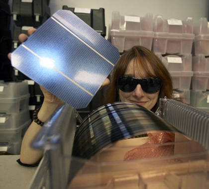
From silicon trash to solar energy: IBM engineers have invented a unique, eco-friendly way to recycle scrap silicon "wafers" -- the base material used for chips in everything from computers to consumer electronics. The new process has dual advantages for the environment, as it will help reduce the estimated 3 million silicon wafers discarded each year across the computer industry, while also providing new supplies of raw materials to the supply-constrained solar energy industry. In this photo James Procopio, an IBM chip manufacturing project manager, holds a semiconductor wafer prior to refurbishment and Michelle Bolz, an IBM manufacturing engineer, displays a solar panel. IBM intends to provide details of the new process to the broader semiconductor manufacturing industry.
Download hi-res version (image/jpeg, 2 MB)
View the associated press release