Saturday, November 15th 2008

Inno3D GeForce 9600 GSO+ Spotted
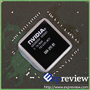
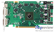
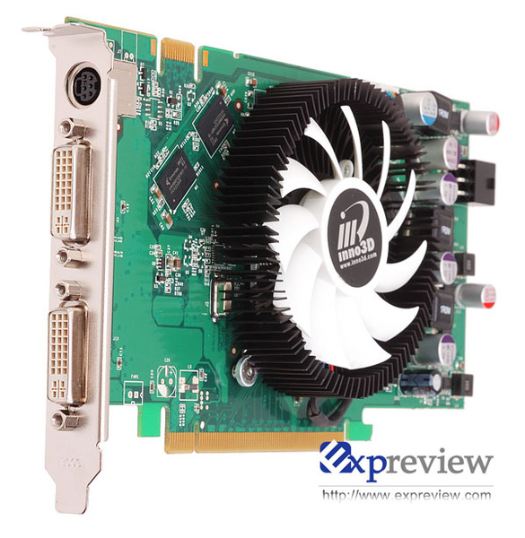
The entry of Radeon HD 4670 did disturb NVIDIA's position, in a segment touted to be one of the cash-cow segments for both NVIDIA and AMD. It is to counter the HD 4870 in its price-range (by easing production-costs), that NVIDIA released a refreshed GeForce 9600 GSO+. The die on the GPU reads "G94-201-B1", pointing that the GPU uses the 55nm silicon fab process (9600 GSO used G92). With the reduced transistor-count on the G94 core, manufacturing the chip becomes cheaper. The real change however, is that NVIDIA made some significant changes to its shader and memory domains, hence the use of G94 core.
The shader count has been reduced from 96 on the 9600 GSO, to 48. This, by disabling 16 shaders from the G94 core. The core is clocked at 650/1675 MHz (core/shader). The GPU is allowed to use the complete width of its memory bus: 256-bit GDDR3. The card features 512 MB of memory, clocked at 1800 MHz. The memory chips featured on the Inno3D card are made by Qimonda, and have a 1.2 ns latency. The card uses a simplistic circular cooler for the GPU. It is expected to be priced at US $87.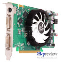
Source:
Expreview
The shader count has been reduced from 96 on the 9600 GSO, to 48. This, by disabling 16 shaders from the G94 core. The core is clocked at 650/1675 MHz (core/shader). The GPU is allowed to use the complete width of its memory bus: 256-bit GDDR3. The card features 512 MB of memory, clocked at 1800 MHz. The memory chips featured on the Inno3D card are made by Qimonda, and have a 1.2 ns latency. The card uses a simplistic circular cooler for the GPU. It is expected to be priced at US $87.


35 Comments on Inno3D GeForce 9600 GSO+ Spotted
And the prospect of this card bores me. lol.
thats the cooler they come with but that OC was on water, 900-2200-2250 is stable for gaming benching all day :D
but 900/2250 is crazy
48 sp's isn't much but definitely enough, not to mention being a 55nm part, with some disabled portions... this card should clock up sommin' fierce.
This is how I see nVidia's naming scheme should be:
8800GT(G80-96SP, what we know as the 8800GTS)
8800GTS(G80-112SP, what we know as the 8800GTS 112)
8800GTX(G80-128SP)
8800Ultra(G80-128SP)
8700GS(G94-48SP, what we know as the new 9600GSO+)
8700GT(G94-64SP, what we know as the 9600GT)
8850GS(G92-96SP, what we know as the 8800GS/9600GSO)
8850GT(G92-112SP, what we know as the 8800GT)
8850GTX(G92-128SP, what we know as the 8800GTS 512MB)
8850Ultra(G92-128SP, what we know as the 9800GTX)
9800GT(GT200-192SP, what we know as the GTX260)
9800GTS(GT200-216SP, what we know as the GTX260 216)
9800GTX(GT200-240SP, what we know as the GTX280)