
2
Cores
2
Threads
35 W
TDP
2000 MHz
Frequency
N/A
Boost
Arrandale
Codename
Socket G1
Socket

Front

Connectivity
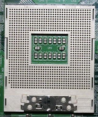
Intel Socket G1
The Intel Pentium P6100 was a mobile processor with 2 cores, launched in September 2010. It is part of the Pentium lineup, using the Arrandale architecture with Socket G1. Pentium P6100 has 3 MB of L3 cache and operates at 2000 MHz. Intel is building the Pentium P6100 on a 32 nm production process using 384 million transistors. The multiplier is locked on Pentium P6100, which limits its overclocking capabilities.
With a TDP of 35 W, the Pentium P6100 consumes only little energy. Intel's processor supports DDR3 memory. For communication with other components in the system, Pentium P6100 uses a PCI-Express Gen 2 connection.
The SSE4 instruction set is not supported, which can cause problems with modern games, as they require that capability.
Physical
| Socket: | Intel Socket G1 |
|---|---|
| Foundry: | Intel |
| Process Size: | 32 nm |
| Transistors: | 384 million |
| Die Size: | 81 mm² |
| Package: | rPGA |
Processor
| Market: | Mobile |
|---|---|
| Production Status: | End-of-life |
| Release Date: | Sep 26th, 2010 |
| Part#: | SLBUR |
Performance
| Frequency: | 2000 MHz |
|---|---|
| Turbo Clock: | N/A |
| Base Clock: | 133 MHz |
| Multiplier: | 15.0x |
| Multiplier Unlocked: | No |
| TDP: | 35 W |
Architecture
| Codename: | Arrandale |
|---|---|
| Generation: |
Pentium
(Arrandale) |
| Memory Support: | DDR3 |
| ECC Memory: | No |
| PCI-Express: | Gen 2 |
Core Config
| # of Cores: | 2 |
|---|---|
| # of Threads: | 2 |
| SMP # CPUs: | 1 |
| Integrated Graphics: | On certain motherboards (Chipset feature) |
Cache
| Cache L1: | 64 KB (per core) |
|---|---|
| Cache L2: | 256 KB (per core) |
| Cache L3: | 3 MB (shared) |
Features
|
Notes
| 177M GPU Transistors |
Apr 25th, 2024 09:37 EDT
change timezone
Latest GPU Drivers
New Forum Posts
- How to quickly & easily fix coil-whine(coil choke noise) (859)
- Asrock A770 Firmware (1)
- RTX 4070 vs RTX 4070 Ti power scaling (5)
- i7-12800HX Overheating Issues (2)
- (Anti) SFF fun house (354)
- What's your latest tech purchase? (20339)
- Alphacool CORE 1 CPU block - bulging with danger of splitting? (6)
- Bizarre Throttlestop issue (6)
- Core i5-6300U (17)
- Last game you purchased? (255)
Popular Reviews
- Fractal Design Terra Review
- Thermalright Phantom Spirit 120 EVO Review
- Corsair 2000D Airflow Review
- Minisforum EliteMini UM780 XTX (AMD Ryzen 7 7840HS) Review
- ASUS GeForce RTX 4090 STRIX OC Review
- NVIDIA GeForce RTX 4090 Founders Edition Review - Impressive Performance
- ASUS GeForce RTX 4090 Matrix Platinum Review - The RTX 4090 Ti
- MSI GeForce RTX 4090 Suprim X Review
- MSI GeForce RTX 4090 Gaming X Trio Review
- Gigabyte GeForce RTX 4090 Gaming OC Review
Controversial News Posts
- Sony PlayStation 5 Pro Specifications Confirmed, Console Arrives Before Holidays (116)
- NVIDIA Points Intel Raptor Lake CPU Users to Get Help from Intel Amid System Instability Issues (106)
- AMD "Strix Halo" Zen 5 Mobile Processor Pictured: Chiplet-based, Uses 256-bit LPDDR5X (101)
- US Government Wants Nuclear Plants to Offload AI Data Center Expansion (98)
- Windows 11 Now Officially Adware as Microsoft Embeds Ads in the Start Menu (88)
- Developers of Outpost Infinity Siege Recommend Underclocking i9-13900K and i9-14900K for Stability on Machines with RTX 4090 (85)
- Windows 10 Security Updates to Cost $61 After 2025, $427 by 2028 (84)
- AMD's RDNA 4 GPUs Could Stick with 18 Gbps GDDR6 Memory (82)