
8
Cores
8
Threads
95 W
TDP
2.8 GHz
Frequency
3.7 GHz
Boost
Zambezi
Codename
Socket AM3+
Socket

Front

Connectivity
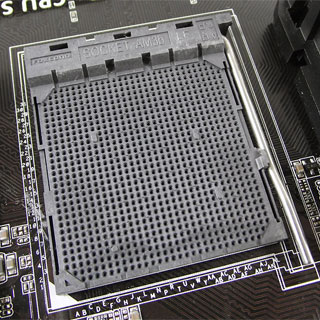
AMD Socket AM3+
The AMD FX-8100 was a desktop processor with 8 cores, launched in October 2011. It is part of the FX lineup, using the Zambezi architecture with Socket AM3+. FX-8100 has 8 MB of L3 cache and operates at 2.8 GHz by default, but can boost up to 3.7 GHz, depending on the workload. AMD is making the FX-8100 on a 32 nm production node using 1,200 million transistors. You may freely adjust the unlocked multiplier on FX-8100, which simplifies overclocking greatly, as you can easily dial in any overclocking frequency.
With a TDP of 95 W, the FX-8100 consumes a good deal of power, so decent cooling is needed. AMD's processor supports DDR3 memory with a dual-channel interface. For communication with other components in the machine, FX-8100 uses a PCI-Express Gen 2 connection. Although the processor doesn't come with integrated graphics, certain motherboards with compatible chipsets can provide this capability.
Hardware virtualization is available on the FX-8100, which greatly improves virtual machine performance. Programs using Advanced Vector Extensions (AVX) can run on this processor, boosting performance for calculation-heavy applications.
Physical
| Socket: | AMD Socket AM3+ |
|---|---|
| Process Size: | 32 nm |
| Transistors: | 1,200 million |
| Die Size: | 315 mm² |
| Package: | µPGA |
Processor
| Market: | Desktop |
|---|---|
| Production Status: | End-of-life |
| Release Date: | Oct 12th, 2011 |
| Part#: | FD8100WMW8KGU |
Performance
| Frequency: | 2.8 GHz |
|---|---|
| Turbo Clock: | up to 3.7 GHz |
| Base Clock: | 200 MHz |
| Multiplier: | 14.0x |
| Multiplier Unlocked: | Yes |
| Voltage: | 1.425 V |
| TDP: | 95 W |
Architecture
| Codename: | Zambezi |
|---|---|
| Generation: |
FX
(Zambezi) |
| Memory Support: | DDR3 |
| Memory Bus: | Dual-channel |
| ECC Memory: | No |
| PCI-Express: | Gen 2 |
Core Config
| # of Cores: | 8 |
|---|---|
| # of Threads: | 8 |
| SMP # CPUs: | 1 |
| Integrated Graphics: | On certain motherboards (Chipset feature) |
Cache
| Cache L1: | 384 KB |
|---|---|
| Cache L2: | 8 MB |
| Cache L3: | 8 MB (shared) |
Features
|
Notes
| 16KB L1 data cache per core. 64KB L1 instruction cache shared per two cores (per module). 2MB L2 cache shared per two cores (per module). This processor comes with an unlocked multiplier, allowing users to set the multiplier value higher than the shipped value, to facilitate better overclocking. |
Apr 24th, 2024 16:34 EDT
change timezone
Latest GPU Drivers
New Forum Posts
- im new to throttelstop and i think i messed it up by copying others any hints would be very much aprreciated (0)
- Is It The 1080 TI The Best GPU Ever? (214)
- What phone you use as your daily driver? And, a discussion of them. (1470)
- Core PL1 + GPU PL1 + Ring EDP OTHER (6)
- Meta Horizon OS (13)
- Rare GPUs / Unreleased GPUs (1875)
- What's your latest tech purchase? (20336)
- What are you playing? (20524)
- Is there a way to have 2x chrome tabs side by side in fullscreen mode? (9)
- Embracer Group is breaking into 3 smaller companies... lol who saw this coming, what a joke (11)
Popular Reviews
- Fractal Design Terra Review
- Thermalright Phantom Spirit 120 EVO Review
- Corsair 2000D Airflow Review
- Minisforum EliteMini UM780 XTX (AMD Ryzen 7 7840HS) Review
- ASUS GeForce RTX 4090 STRIX OC Review
- NVIDIA GeForce RTX 4090 Founders Edition Review - Impressive Performance
- ASUS GeForce RTX 4090 Matrix Platinum Review - The RTX 4090 Ti
- MSI GeForce RTX 4090 Gaming X Trio Review
- MSI GeForce RTX 4090 Suprim X Review
- Gigabyte GeForce RTX 4090 Gaming OC Review
Controversial News Posts
- Sony PlayStation 5 Pro Specifications Confirmed, Console Arrives Before Holidays (116)
- NVIDIA Points Intel Raptor Lake CPU Users to Get Help from Intel Amid System Instability Issues (106)
- AMD "Strix Halo" Zen 5 Mobile Processor Pictured: Chiplet-based, Uses 256-bit LPDDR5X (101)
- US Government Wants Nuclear Plants to Offload AI Data Center Expansion (98)
- Windows 10 Security Updates to Cost $61 After 2025, $427 by 2028 (84)
- Developers of Outpost Infinity Siege Recommend Underclocking i9-13900K and i9-14900K for Stability on Machines with RTX 4090 (84)
- TechPowerUp Hiring: Reviewers Wanted for Motherboards, Laptops, Gaming Handhelds and Prebuilt Desktops (78)
- Intel Realizes the Only Way to Save x86 is to Democratize it, Reopens x86 IP Licensing (70)