• Welcome to TechPowerUp Forums, Guest! Please check out our forum guidelines for info related to our community.

IBM Creates 9 nm Transistors Using Carbon Nanotubules

btarunr

Editor & Senior Moderator
Staff member
Joined
Oct 9, 2007
Messages
46,355 (7.68/day)
Location
Hyderabad, India
System Name RBMK-1000
Processor AMD Ryzen 7 5700G
Motherboard ASUS ROG Strix B450-E Gaming
Cooling DeepCool Gammax L240 V2
Memory 2x 8GB G.Skill Sniper X
Video Card(s) Palit GeForce RTX 2080 SUPER GameRock
Storage Western Digital Black NVMe 512GB
Display(s) BenQ 1440p 60 Hz 27-inch
Case Corsair Carbide 100R
Audio Device(s) ASUS SupremeFX S1220A
Power Supply Cooler Master MWE Gold 650W
Mouse ASUS ROG Strix Impact
Keyboard Gamdias Hermes E2
Software Windows 11 Pro
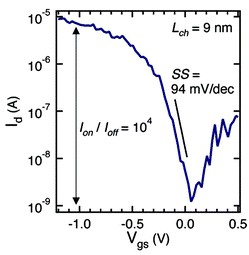
Researchers at IBM have developed the smallest carbon nanotubule transistor, that is 9 nanometers (nm) across. In comparison, the smallest transistors possible using silicon is 10 nm across. IBM claims its new transistor consumes less power while being able to carry more current than today's technology.

"The results really highlight the value of nanotubes in the most sophisticated type of transistors," says John Rogers, professor of materials science at the University of Illinois at Urbana-Champaign. "They suggest, very clearly, that nanotubes have the potential for doing something truly competitive with, or complementary to, silicon." Currently, the smallest production-grade transistors are 22 nm across.


The success of 9 nm carbon nanotubule transistors potentially extends the life of conventional electronics as we know it, as it breaches the 10 nm limit of silicon transistors. "If nanotubes can't go much further than silicon, then working on them is a waste of time," says Aaron Franklin, a researcher at the IBM Watson Research Center in Yorktown Heights, New York. "We've made nanotube transistors at aggressively scaled dimensions, and shown they are tremendously better than the best silicon devices." The research team, however, is faced with development hurdles. Manufacturing large batches of carbon nanotubules that function as semiconductors is difficult.

View at TechPowerUp Main Site
 

Completely Bonkers

New Member
Joined
Feb 6, 2007
Messages
2,576 (0.41/day)
Processor Mysterious Engineering Prototype
Motherboard Intel 865
Cooling Custom block made in workshop
Memory Corsair XMS 2GB
Video Card(s) FireGL X3-256
Display(s) 1600x1200 SyncMaster x 2 = 3200x1200
Software Windows 2003
I'm less interested about 9nm vs 12/15nm silicon, than about switching speeds and current leakage. If carbon nanotube transistors can switch faster than silicon or can run at lower power/heat loss, then they are a win irrespective of scaling to a smaller size.
 
Joined
Sep 1, 2010
Messages
7,023 (1.41/day)
Nice. Carbon nanotube is graphene rolled up in a tube. Theoretically that thing's limit is ~ 3 nm or something. So maybe oneday we'll get 3 nm technology. Still a long way to go to get to quantum tunnelling (1 nm and smaller)
 

R_1

Joined
Dec 1, 2006
Messages
448 (0.07/day)
Yes, but those carbon nanotubes are grown separately and then embedded on a substrate with some fancy manipulator. It probably can build one transistor at a time, so 2 billion of them should take long time to assemble.
 

Benetanegia

New Member
Joined
Sep 11, 2009
Messages
2,680 (0.50/day)
Location
Reaching your left retina.
I'm less interested about 9nm vs 12/15nm silicon, than about switching speeds and current leakage. If carbon nanotube transistors can switch faster than silicon or can run at lower power/heat loss, then they are a win irrespective of scaling to a smaller size.

I agree, but last time I checked and iirc they were only able to create carbon nanotube structures the size of hundreds of nm. I don't rememer the actual size, but I do remember the difference was so big compared to current silicon processes that they were not small enough to create anything even close to a modern processor, of any type. The fact they have been able to catch up or even surpass silicon is amazing.
 
Joined
Oct 30, 2008
Messages
1,758 (0.31/day)
System Name Lailalo
Processor Ryzen 9 5900X Boosts to 4.95Ghz
Motherboard Asus TUF Gaming X570-Plus (WIFI
Cooling Noctua
Memory 32GB DDR4 3200 Corsair Vengeance
Video Card(s) XFX 7900XT 20GB
Storage Samsung 970 Pro Plus 1TB, Crucial 1TB MX500 SSD, Segate 3TB
Display(s) LG Ultrawide 29in @ 2560x1080
Case Coolermaster Storm Sniper
Power Supply XPG 1000W
Mouse G602
Keyboard G510s
Software Windows 10 Pro / Windows 10 Home
If it advances us towards Chobits then I say...DO EEET!!!!!! :D
 

Benetanegia

New Member
Joined
Sep 11, 2009
Messages
2,680 (0.50/day)
Location
Reaching your left retina.
Yes, but those carbon nanotubes are grown separately and then embedded on a substrate with some fancy manipulator. It probably can build one transistor at a time, so 2 billion of them should take long time to assemble.

lol they will not create them one by one. Far from it. They already demostrated a working RF chip 1-2 years ago, created with existent silicon manufacturing equipment. So on one hand they can already create them with the same process that silicon transistors are made, but those are/were large*. On the other hand, they can create 9 nm ones "one by one" (not really though) and have demostrated their viability/superiority and that it's posible to go smaller. At some point, soon hpefully, the two technologies will converge into something usable.

* Considering they were using very old equipment it's posible that they could go smaller than what they did, only that's the equipment they used back then.
 
Joined
Nov 4, 2005
Messages
11,681 (1.73/day)
System Name Compy 386
Processor 7800X3D
Motherboard Asus
Cooling Air for now.....
Memory 64 GB DDR5 6400Mhz
Video Card(s) 7900XTX 310 Merc
Storage Samsung 990 2TB, 2 SP 2TB SSDs and over 10TB spinning
Display(s) 56" Samsung 4K HDR
Audio Device(s) ATI HDMI
Mouse Logitech MX518
Keyboard Razer
Software A lot.
Benchmark Scores Its fast. Enough.
There is always a breakthrough at the right wrong time, just like there was with doped silicon. Hopefully one of these advancements will pan out to be the next greatest thing.
 

WarraWarra

New Member
Joined
Nov 23, 2010
Messages
268 (0.05/day)
Beautiful finally IBM gets it, bit late but finally. :toast:

Okay next step is to use the protein based nano tubes material that doubles as heatsink if used as pcboard material, aluminum replacement, space construction material (that can be produced on demand and scaled during space travel) to build 3D nano tube grids similar to Intel tri-gate just not as primitive.

I guess I have to spoon feed even this to Intel and IBM again :banghead:

O well .....
 
Top