Report an Error


NVIDIA GeForce 6800 Ultra
- Graphics Processor
- NV40
- Pixel Shaders
- 16
- Vertex Shaders
- 6
- TMUs
- 16
- ROPs
- 16
- Memory Size
- 256 MB
- Memory Type
- GDDR3
- Bus Width
- 256 bit

GPU
Recommended Gaming Resolutions:
- 640x480
- 1280x720
- 1366x768
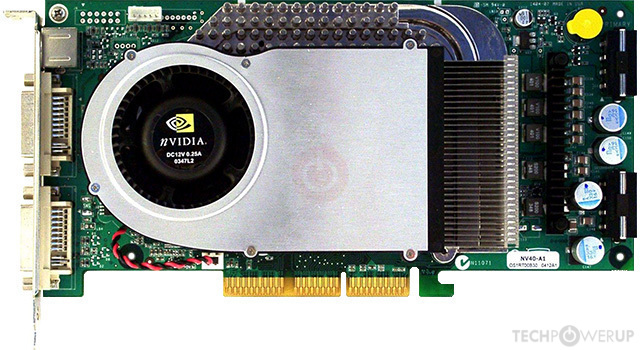
The GeForce 6800 Ultra was a graphics card by NVIDIA, launched on April 14th, 2004. Built on the 130 nm process, and based on the NV40 graphics processor, in its 6800 Ultra variant, the card supports DirectX 9.0c. Since GeForce 6800 Ultra does not support DirectX 11 or DirectX 12, it might not be able to run all the latest games. The NV40 graphics processor is an average sized chip with a die area of 287 mm² and 222 million transistors. It features 16 pixel shaders and 6 vertex shaders, 16 texture mapping units, and 16 ROPs. Due to the lack of unified shaders you will not be able to run recent games at all (which require unified shader/DX10+ support). NVIDIA has paired 256 MB GDDR3 memory with the GeForce 6800 Ultra, which are connected using a 256-bit memory interface. The GPU is operating at a frequency of 425 MHz, memory is running at 550 MHz.
Being a single-slot card, the NVIDIA GeForce 6800 Ultra draws power from 2x Molex power connectors, with power draw not exactly known. Display outputs include: 2x DVI, 1x S-Video. GeForce 6800 Ultra is connected to the rest of the system using an AGP 8x interface. The card measures 216 mm in length, and features a single-slot cooling solution.
Being a single-slot card, the NVIDIA GeForce 6800 Ultra draws power from 2x Molex power connectors, with power draw not exactly known. Display outputs include: 2x DVI, 1x S-Video. GeForce 6800 Ultra is connected to the rest of the system using an AGP 8x interface. The card measures 216 mm in length, and features a single-slot cooling solution.
Graphics Processor
Graphics Card
- Release Date
- Apr 14th, 2004
- Generation
-
GeForce 6 AGP
(6800)
- Predecessor
- GeForce FX
- Successor
- GeForce 7 AGP
- Production
- End-of-life
- Bus Interface
- AGP 8x
- Reviews
- 115 in our database
Clock Speeds
- GPU Clock
- 425 MHz
- Memory Clock
-
550 MHz
1100 Mbps effective
Memory
- Memory Size
- 256 MB
- Memory Type
- GDDR3
- Memory Bus
- 256 bit
- Bandwidth
- 35.20 GB/s
Render Config
- Pixel Shaders
- 16
- Vertex Shaders
- 6
- TMUs
- 16
- ROPs
- 16
Theoretical Performance
- Pixel Rate
- 6.800 GPixel/s
- Vertex Rate
- 637.5 MVertices/s
- Texture Rate
- 6.800 GTexel/s
Board Design
- Slot Width
- Single-slot
- Length
- 216 mm
8.5 inches
- TDP
- unknown
- Suggested PSU
- 200 W
- Outputs
- 2x DVI
1x S-Video
- Power Connectors
- 2x Molex
- Board Number
- P201
Graphics Features
- DirectX
- 9.0c (9_3)
- OpenGL
-
2.0 (full)
2.1 (partial)
- OpenCL
- N/A
- Vulkan
- N/A
- Shader Model
- 3.0
NV40 GPU Notes
| PureVideo HD: VP1 VDPAU: No Support |
Retail boards based on this design (4)
| Name | GPU Clock | Memory Clock | Other Changes |
|---|---|---|---|
| 425 MHz | 550 MHz | Dual-slot | |
| 425 MHz | 550 MHz | ||
| 450 MHz | 600 MHz | ||
| 425 MHz | 550 MHz |


Apr 24th, 2024 21:38 EDT
change timezone
Latest GPU Drivers
New Forum Posts
- (Anti) SFF fun house (347)
- Cinebench crashed my PC. My Wi-Fi stopped working, and I keep getting a "Please wait" screen when I boot up my PC. (30)
- The TPU UK Clubhouse (24783)
- Sharing experience with MSI RTX 3070 vBIOS update to enable Resizable Bar with MB Z490 (2)
- Share your AIDA 64 cache and memory benchmark here (2915)
- Will a RTX 4070 TI super bottleneck a Ryzen 9 7950X3D? (58)
- The best *budget* ATX PC case on the market? (24)
- GTX 1070 Ti - TDP Issues - Always Power Throttling (4)
- 2022-X58/1366 PIN Motherboards NVME M.2 SSD BIOS MOD Collection (656)
- Meta Horizon OS (15)
Popular Reviews
- Fractal Design Terra Review
- Thermalright Phantom Spirit 120 EVO Review
- Corsair 2000D Airflow Review
- Minisforum EliteMini UM780 XTX (AMD Ryzen 7 7840HS) Review
- ASUS GeForce RTX 4090 STRIX OC Review
- NVIDIA GeForce RTX 4090 Founders Edition Review - Impressive Performance
- ASUS GeForce RTX 4090 Matrix Platinum Review - The RTX 4090 Ti
- MSI GeForce RTX 4090 Suprim X Review
- MSI GeForce RTX 4090 Gaming X Trio Review
- Gigabyte GeForce RTX 4090 Gaming OC Review
Controversial News Posts
- Sony PlayStation 5 Pro Specifications Confirmed, Console Arrives Before Holidays (116)
- NVIDIA Points Intel Raptor Lake CPU Users to Get Help from Intel Amid System Instability Issues (106)
- AMD "Strix Halo" Zen 5 Mobile Processor Pictured: Chiplet-based, Uses 256-bit LPDDR5X (101)
- US Government Wants Nuclear Plants to Offload AI Data Center Expansion (98)
- Windows 10 Security Updates to Cost $61 After 2025, $427 by 2028 (84)
- Developers of Outpost Infinity Siege Recommend Underclocking i9-13900K and i9-14900K for Stability on Machines with RTX 4090 (84)
- TechPowerUp Hiring: Reviewers Wanted for Motherboards, Laptops, Gaming Handhelds and Prebuilt Desktops (78)
- AMD's RDNA 4 GPUs Could Stick with 18 Gbps GDDR6 Memory (73)