Report an Error


NVIDIA Quadro FX 4500 X2
- Graphics Processor
- G71 x2
- Pixel Shaders
- 24 x2
- Vertex Shaders
- 8 x2
- TMUs
- 24 x2
- ROPs
- 16 x2
- Memory Size
- 512 MB x2
- Memory Type
- GDDR3
- Bus Width
- 256 bit x2

GPU
Recommended Gaming Resolutions:
- 1280x720
- 1366x768
- 1600x900
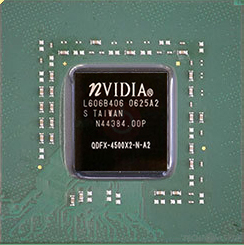
The Quadro FX 4500 X2 was an enthusiast-class professional graphics card by NVIDIA, launched on April 24th, 2006. Built on the 90 nm process, and based on the G71 graphics processor, in its QDFX-4500X2-N-A2 variant, the card supports DirectX 9.0c. Since Quadro FX 4500 X2 does not support DirectX 11 or DirectX 12, it might not be able to run all the latest games. The G71 graphics processor is an average sized chip with a die area of 196 mm² and 278 million transistors. Quadro FX 4500 X2 combines two graphics processors to increase performance. It features 24 pixel shaders and 8 vertex shaders, 24 texture mapping units, and 16 ROPs, per GPU. Due to the lack of unified shaders you will not be able to run recent games at all (which require unified shader/DX10+ support). NVIDIA has paired 1,024 MB GDDR3 memory with the Quadro FX 4500 X2, which are connected using a 256-bit memory interface per GPU (each GPU manages 512 MB). The GPU is operating at a frequency of 500 MHz, memory is running at 605 MHz.
Being a dual-slot card, the NVIDIA Quadro FX 4500 X2 draws power from 2x 6-pin power connectors, with power draw rated at 145 W maximum. Display outputs include: 4x DVI. Quadro FX 4500 X2 is connected to the rest of the system using a PCI-Express 1.0 x16 interface. The card measures 305 mm in length, 111 mm in width, and features a dual-slot cooling solution. Its price at launch was 2799 US Dollars.
Being a dual-slot card, the NVIDIA Quadro FX 4500 X2 draws power from 2x 6-pin power connectors, with power draw rated at 145 W maximum. Display outputs include: 4x DVI. Quadro FX 4500 X2 is connected to the rest of the system using a PCI-Express 1.0 x16 interface. The card measures 305 mm in length, 111 mm in width, and features a dual-slot cooling solution. Its price at launch was 2799 US Dollars.
Graphics Processor
Graphics Card
- Release Date
- Apr 24th, 2006
- Generation
-
Quadro FX Curie
(x500)
- Predecessor
- Quadro FX Rankine
- Successor
- Quadro FX Tesla
- Production
- End-of-life
- Launch Price
- 2,799 USD
- Bus Interface
- PCIe 1.0 x16
- Reviews
- 26 in our database
Clock Speeds
- GPU Clock
- 500 MHz
- Memory Clock
-
605 MHz
1210 Mbps effective
Memory
- Memory Size
- 512 MB
- Memory Type
- GDDR3
- Memory Bus
- 256 bit
- Bandwidth
- 38.72 GB/s
Render Config
- Pixel Shaders
- 24
- Vertex Shaders
- 8
- TMUs
- 24
- ROPs
- 16
Theoretical Performance
- Pixel Rate
- 8.000 GPixel/s
- Vertex Rate
- 1.000 GVertices/s
- Texture Rate
- 12.00 GTexel/s
Board Design
- Slot Width
- Dual-slot
- Length
- 305 mm
12 inches
- Width
- 111 mm
4.4 inches
- TDP
- 145 W
- Suggested PSU
- 300 W
- Outputs
- 4x DVI
- Power Connectors
- 2x 6-pin
- Board Number
- Q278 SKU 501
Graphics Features
- DirectX
- 9.0c (9_3)
- OpenGL
- 2.1
- OpenCL
- N/A
- Vulkan
- N/A
- Shader Model
- 3.0
G71 GPU Notes
| PureVideo HD: VP1 VDPAU: No Support |
Apr 19th, 2024 15:49 EDT
change timezone
Latest GPU Drivers
New Forum Posts
- XFX RX560 1024 shaders 16 CU 4GB from Aliexpress (10)
- [WIN11] 5700x3d Security processor Attestation: Not supported? (6)
- DDR5 RAM Speeds and the future (51)
- What are you playing? (20468)
- Linus watercools (46)
- Identify my GPU - RX 570 8GB (or what?) (6)
- Will a RTX 4070 TI super bottleneck a Ryzen 9 7950X3D? (39)
- Is it possible to use Linux without the Terminal/command line? (27)
- Which air cooler for a ryzen 9 5900x (160)
- Which terminal emulator do you use the most? (9)
Popular Reviews
- Horizon Forbidden West Performance Benchmark Review - 30 GPUs Tested
- PowerColor Radeon RX 7900 GRE Hellhound Review
- Fractal Design Terra Review
- Corsair 2000D Airflow Review
- Thermalright Phantom Spirit 120 EVO Review
- Minisforum EliteMini UM780 XTX (AMD Ryzen 7 7840HS) Review
- Creative Pebble X Plus Review
- FiiO KB3 HiFi Mechanical Keyboard Review - Integrated DAC/Amp!
- ASUS GeForce RTX 4090 STRIX OC Review
- NVIDIA GeForce RTX 4090 Founders Edition Review - Impressive Performance
Controversial News Posts
- Sony PlayStation 5 Pro Specifications Confirmed, Console Arrives Before Holidays (110)
- NVIDIA Points Intel Raptor Lake CPU Users to Get Help from Intel Amid System Instability Issues (102)
- US Government Wants Nuclear Plants to Offload AI Data Center Expansion (98)
- Windows 10 Security Updates to Cost $61 After 2025, $427 by 2028 (82)
- Developers of Outpost Infinity Siege Recommend Underclocking i9-13900K and i9-14900K for Stability on Machines with RTX 4090 (82)
- AMD "Strix Halo" Zen 5 Mobile Processor Pictured: Chiplet-based, Uses 256-bit LPDDR5X (76)
- TechPowerUp Hiring: Reviewers Wanted for Motherboards, Laptops, Gaming Handhelds and Prebuilt Desktops (72)
- Intel Realizes the Only Way to Save x86 is to Democratize it, Reopens x86 IP Licensing (70)