Report an Error


NVIDIA Quadro 5010M
- Graphics Processor
- GF110
- Cores
- 384
- TMUs
- 48
- ROPs
- 32
- Memory Size
- 4 GB
- Memory Type
- GDDR5
- Bus Width
- 256 bit

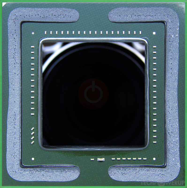
GPU
Recommended Gaming Resolutions:
- 1366x768
- 1600x900
- 1920x1080
The Quadro 5010M was a professional mobile graphics chip by NVIDIA, launched on February 22nd, 2011. Built on the 40 nm process, and based on the GF110 graphics processor, in its N12E-Q5-A1 variant, the chip supports DirectX 12. The GF110 graphics processor is a large chip with a die area of 520 mm² and 3,000 million transistors. Unlike the fully unlocked GeForce GTX 580, which uses the same GPU but has all 512 shaders enabled, NVIDIA has disabled some shading units on the Quadro 5010M to reach the product's target shader count. It features 384 shading units, 48 texture mapping units, and 32 ROPs. NVIDIA has paired 4 GB GDDR5 memory with the Quadro 5010M, which are connected using a 256-bit memory interface. The GPU is operating at a frequency of 450 MHz, memory is running at 650 MHz (2.6 Gbps effective).
Being a mxm module card, the NVIDIA Quadro 5010M does not require any additional power connector, its power draw is rated at 100 W maximum. This device has no display connectivity, as it is not designed to have monitors connected to it. Rather it is intended for use in laptop/notebooks and will use the output of the host mobile device.
Being a mxm module card, the NVIDIA Quadro 5010M does not require any additional power connector, its power draw is rated at 100 W maximum. This device has no display connectivity, as it is not designed to have monitors connected to it. Rather it is intended for use in laptop/notebooks and will use the output of the host mobile device.
Graphics Processor
Mobile Graphics
- Release Date
- Feb 22nd, 2011
- Generation
-
Quadro Fermi-M
(x000M)
- Predecessor
- Quadro FX Mobile
- Successor
- Quadro Kepler-M
- Production
- End-of-life
- Bus Interface
- MXM-B (3.0)
- Reviews
- 26 in our database
Relative Performance
Based on TPU review data: "Performance Summary" at 1920x1080, 4K for 2080 Ti and faster.
Performance estimated based on architecture, shader count and clocks.
Clock Speeds
- GPU Clock
- 450 MHz
- Shader Clock
- 900 MHz
- Memory Clock
-
650 MHz
2.6 Gbps effective
Memory
- Memory Size
- 4 GB
- Memory Type
- GDDR5
- Memory Bus
- 256 bit
- Bandwidth
- 83.20 GB/s
Render Config
- Shading Units
- 384
- TMUs
- 48
- ROPs
- 32
- SM Count
- 12
- L1 Cache
- 64 KB (per SM)
- L2 Cache
- 512 KB
Theoretical Performance
- Pixel Rate
- 10.80 GPixel/s
- Texture Rate
- 21.60 GTexel/s
- FP32 (float)
- 691.2 GFLOPS
Board Design
- Slot Width
- MXM Module
- TDP
- 100 W
- Outputs
- Portable Device Dependent
- Power Connectors
- None
- Board Number
- P1347 SKU 501
Graphics Features
- DirectX
- 12 (11_0)
- OpenGL
- 4.6
- OpenCL
- 1.1
- Vulkan
- N/A
- CUDA
- 2.0
- Shader Model
- 5.1
GF110 GPU Notes
| PureVideo HD: VP4 VDPAU: Feature Set C GF110 has 4 GPCs each capable of 8 pixels per clock. This limits complete GPU to 32 pixels per clock and because of that it can't feed all 48 ROPs when they all require data at the same time. Additional ROPs however can be used for MSAA (because it doesn't require additional data from rasterizers, while giving more work to ROPs.) The complete die contains 64 texture address units and 256 texture filtering units. |
Apr 23rd, 2024 16:35 EDT
change timezone
Latest GPU Drivers
New Forum Posts
- CPB Enabled Boot Loop (4)
- Aida64 cache mem OC (4)
- No POST, and no display (7)
- Meta Horizon OS (6)
- windows 11 (4)
- Which new games will you be buying? (299)
- need help with motherboard/ ram compability certainty (5)
- My computer setup - Request for opinions (11)
- EK seems to be having major issues (26)
- DeepCool AIO LS720 RGB NOT WORKING HELP! (0)
Popular Reviews
- Horizon Forbidden West Performance Benchmark Review - 30 GPUs Tested
- Fractal Design Terra Review
- Corsair 2000D Airflow Review
- Thermalright Phantom Spirit 120 EVO Review
- Minisforum EliteMini UM780 XTX (AMD Ryzen 7 7840HS) Review
- ASUS GeForce RTX 4090 STRIX OC Review
- NVIDIA GeForce RTX 4090 Founders Edition Review - Impressive Performance
- ASUS GeForce RTX 4090 Matrix Platinum Review - The RTX 4090 Ti
- Creative Pebble X Plus Review
- MSI GeForce RTX 4090 Gaming X Trio Review
Controversial News Posts
- Sony PlayStation 5 Pro Specifications Confirmed, Console Arrives Before Holidays (116)
- NVIDIA Points Intel Raptor Lake CPU Users to Get Help from Intel Amid System Instability Issues (105)
- AMD "Strix Halo" Zen 5 Mobile Processor Pictured: Chiplet-based, Uses 256-bit LPDDR5X (101)
- US Government Wants Nuclear Plants to Offload AI Data Center Expansion (98)
- Windows 10 Security Updates to Cost $61 After 2025, $427 by 2028 (84)
- Developers of Outpost Infinity Siege Recommend Underclocking i9-13900K and i9-14900K for Stability on Machines with RTX 4090 (84)
- TechPowerUp Hiring: Reviewers Wanted for Motherboards, Laptops, Gaming Handhelds and Prebuilt Desktops (74)
- Intel Realizes the Only Way to Save x86 is to Democratize it, Reopens x86 IP Licensing (70)