Report an Error


NVIDIA Quadro NVS 320M
- Graphics Processor
- G84
- Cores
- 32
- TMUs
- 16
- ROPs
- 8
- Memory Size
- 512 MB
- Memory Type
- GDDR3
- Bus Width
- 128 bit
GPU
Recommended Gaming Resolutions:
- 640x480
- 1280x720
- 1366x768
The Quadro NVS 320M was a professional mobile graphics chip by NVIDIA, launched on June 9th, 2007. Built on the 80 nm process, and based on the G84 graphics processor, the chip supports DirectX 11.1. Even though it supports DirectX 11, the feature level is only 10_0, which can be problematic with many DirectX 11 & DirectX 12 titles. The G84 graphics processor is an average sized chip with a die area of 169 mm² and 289 million transistors. It features 32 shading units, 16 texture mapping units, and 8 ROPs. NVIDIA has paired 512 MB GDDR3 memory with the Quadro NVS 320M, which are connected using a 128-bit memory interface. The GPU is operating at a frequency of 575 MHz, memory is running at 700 MHz.
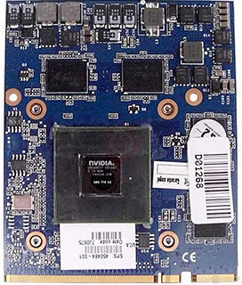
Being a mxm module card, the NVIDIA Quadro NVS 320M does not require any additional power connector, its power draw is rated at 20 W maximum. This device has no display connectivity, as it is not designed to have monitors connected to it. Rather it is intended for use in laptop/notebooks and will use the output of the host mobile device.
Being a mxm module card, the NVIDIA Quadro NVS 320M does not require any additional power connector, its power draw is rated at 20 W maximum. This device has no display connectivity, as it is not designed to have monitors connected to it. Rather it is intended for use in laptop/notebooks and will use the output of the host mobile device.
Graphics Processor
Mobile Graphics
- Release Date
- Jun 9th, 2007
- Generation
- NVS Mobile
- Production
- End-of-life
- Bus Interface
- MXM-HE
- Reviews
- 26 in our database
Relative Performance
Based on TPU review data: "Performance Summary" at 1920x1080, 4K for 2080 Ti and faster.
Performance estimated based on architecture, shader count and clocks.
Clock Speeds
- GPU Clock
- 575 MHz
- Shader Clock
- 1150 MHz
- Memory Clock
-
700 MHz
1400 Mbps effective
Memory
- Memory Size
- 512 MB
- Memory Type
- GDDR3
- Memory Bus
- 128 bit
- Bandwidth
- 22.40 GB/s
Render Config
- Shading Units
- 32
- TMUs
- 16
- ROPs
- 8
- SM Count
- 4
- L2 Cache
- 32 KB
Theoretical Performance
- Pixel Rate
- 4.600 GPixel/s
- Texture Rate
- 9.200 GTexel/s
- FP32 (float)
- 73.60 GFLOPS
Board Design
- Slot Width
- MXM Module
- TDP
- 20 W
- Outputs
- Portable Device Dependent
- Power Connectors
- None
Graphics Features
- DirectX
- 11.1 (10_0)
- OpenGL
- 3.3
- OpenCL
- 1.1
- Vulkan
- N/A
- CUDA
- 1.1
- Shader Model
- 4.0
G84 GPU Notes
| PureVideo HD: VP2 VDPAU: Feature Set A |
Apr 19th, 2024 07:06 EDT
change timezone
Latest GPU Drivers
New Forum Posts
- Should the CDPR make the Fallout 5 instead? (28)
- Can't find rx 580 2048sp vbios (4)
- Do you use Linux? (231)
- What's your latest tech purchase? (20284)
- First computer build for my son (5)
- DDR5 RAM Speeds and the future (46)
- Gelid Offering Odd Inconsistencies - WTF? (1)
- Linus watercools (24)
- I7-8750H + GTX 1050ti Laptop drops performance periodically (0)
- Roccat Kone AIMO has developed a double left click, when I click it once. Any fix out there? (28)
Popular Reviews
- Horizon Forbidden West Performance Benchmark Review - 30 GPUs Tested
- PowerColor Radeon RX 7900 GRE Hellhound Review
- Fractal Design Terra Review
- Corsair 2000D Airflow Review
- Thermalright Phantom Spirit 120 EVO Review
- Minisforum EliteMini UM780 XTX (AMD Ryzen 7 7840HS) Review
- Creative Pebble X Plus Review
- FiiO KB3 HiFi Mechanical Keyboard Review - Integrated DAC/Amp!
- ASUS GeForce RTX 4090 STRIX OC Review
- NVIDIA GeForce RTX 4090 Founders Edition Review - Impressive Performance
Controversial News Posts
- Sony PlayStation 5 Pro Specifications Confirmed, Console Arrives Before Holidays (110)
- NVIDIA Points Intel Raptor Lake CPU Users to Get Help from Intel Amid System Instability Issues (102)
- US Government Wants Nuclear Plants to Offload AI Data Center Expansion (98)
- Windows 10 Security Updates to Cost $61 After 2025, $427 by 2028 (82)
- Developers of Outpost Infinity Siege Recommend Underclocking i9-13900K and i9-14900K for Stability on Machines with RTX 4090 (82)
- TechPowerUp Hiring: Reviewers Wanted for Motherboards, Laptops, Gaming Handhelds and Prebuilt Desktops (71)
- Intel Realizes the Only Way to Save x86 is to Democratize it, Reopens x86 IP Licensing (70)
- AMD Zen 5 Execution Engine Leaked, Features True 512-bit FPU (63)