Report an Error


NVIDIA Tesla M2090
- Graphics Processor
- GF110
- Cores
- 512
- TMUs
- 64
- ROPs
- 48
- Memory Size
- 6 GB
- Memory Type
- GDDR5
- Bus Width
- 384 bit
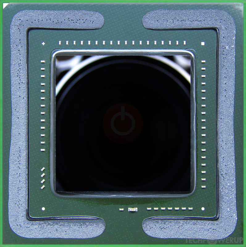
GPU
The Tesla M2090 was a professional graphics card by NVIDIA, launched on July 25th, 2011. Built on the 40 nm process, and based on the GF110 graphics processor, the card supports DirectX 12. The GF110 graphics processor is a large chip with a die area of 520 mm² and 3,000 million transistors. It features 512 shading units, 64 texture mapping units, and 48 ROPs. NVIDIA has paired 6 GB GDDR5 memory with the Tesla M2090, which are connected using a 384-bit memory interface. The GPU is operating at a frequency of 651 MHz, memory is running at 924 MHz (3.7 Gbps effective).
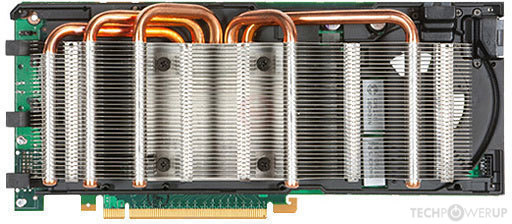
Being a dual-slot card, the NVIDIA Tesla M2090 draws power from 1x 6-pin + 1x 8-pin power connector, with power draw rated at 250 W maximum. This device has no display connectivity, as it is not designed to have monitors connected to it. Tesla M2090 is connected to the rest of the system using a PCI-Express 2.0 x16 interface. The card measures 248 mm in length, and features a dual-slot cooling solution.
Being a dual-slot card, the NVIDIA Tesla M2090 draws power from 1x 6-pin + 1x 8-pin power connector, with power draw rated at 250 W maximum. This device has no display connectivity, as it is not designed to have monitors connected to it. Tesla M2090 is connected to the rest of the system using a PCI-Express 2.0 x16 interface. The card measures 248 mm in length, and features a dual-slot cooling solution.
Graphics Processor
Graphics Card
- Release Date
- Jul 25th, 2011
- Generation
-
Tesla Fermi
(x20xx)
- Predecessor
- Tesla
- Successor
- Tesla Kepler
- Production
- End-of-life
- Bus Interface
- PCIe 2.0 x16
Relative Performance
Based on TPU review data: "Performance Summary" at 1920x1080, 4K for 2080 Ti and faster.
Performance estimated based on architecture, shader count and clocks.
Clock Speeds
- GPU Clock
- 651 MHz
- Shader Clock
- 1301 MHz
- Memory Clock
-
924 MHz
3.7 Gbps effective
Memory
- Memory Size
- 6 GB
- Memory Type
- GDDR5
- Memory Bus
- 384 bit
- Bandwidth
- 177.4 GB/s
Render Config
- Shading Units
- 512
- TMUs
- 64
- ROPs
- 48
- SM Count
- 16
- L1 Cache
- 64 KB (per SM)
- L2 Cache
- 768 KB
Theoretical Performance
- Pixel Rate
- 20.83 GPixel/s
- Texture Rate
- 41.66 GTexel/s
- FP32 (float)
- 1,332 GFLOPS
- FP64 (double)
- 666.1 GFLOPS (1:2)
Board Design
- Slot Width
- Dual-slot
- Length
- 248 mm
9.8 inches
- TDP
- 250 W
- Suggested PSU
- 600 W
- Outputs
- No outputs
- Power Connectors
- 1x 6-pin + 1x 8-pin
- Board Number
- P1030 SKU 214
Graphics Features
- DirectX
- 12 (11_0)
- OpenGL
- 4.6
- OpenCL
- 1.1
- Vulkan
- N/A
- CUDA
- 2.0
- Shader Model
- 5.1
GF110 GPU Notes
| PureVideo HD: VP4 VDPAU: Feature Set C GF110 has 4 GPCs each capable of 8 pixels per clock. This limits complete GPU to 32 pixels per clock and because of that it can't feed all 48 ROPs when they all require data at the same time. Additional ROPs however can be used for MSAA (because it doesn't require additional data from rasterizers, while giving more work to ROPs.) The complete die contains 64 texture address units and 256 texture filtering units. |
Apr 19th, 2024 15:51 EDT
change timezone
Latest GPU Drivers
New Forum Posts
- What are you playing? (20469)
- XFX RX560 1024 shaders 16 CU 4GB from Aliexpress (10)
- [WIN11] 5700x3d Security processor Attestation: Not supported? (6)
- DDR5 RAM Speeds and the future (51)
- Linus watercools (46)
- Identify my GPU - RX 570 8GB (or what?) (6)
- Will a RTX 4070 TI super bottleneck a Ryzen 9 7950X3D? (39)
- Is it possible to use Linux without the Terminal/command line? (27)
- Which air cooler for a ryzen 9 5900x (160)
- Which terminal emulator do you use the most? (9)
Popular Reviews
- Horizon Forbidden West Performance Benchmark Review - 30 GPUs Tested
- PowerColor Radeon RX 7900 GRE Hellhound Review
- Fractal Design Terra Review
- Corsair 2000D Airflow Review
- Thermalright Phantom Spirit 120 EVO Review
- Minisforum EliteMini UM780 XTX (AMD Ryzen 7 7840HS) Review
- Creative Pebble X Plus Review
- FiiO KB3 HiFi Mechanical Keyboard Review - Integrated DAC/Amp!
- ASUS GeForce RTX 4090 STRIX OC Review
- NVIDIA GeForce RTX 4090 Founders Edition Review - Impressive Performance
Controversial News Posts
- Sony PlayStation 5 Pro Specifications Confirmed, Console Arrives Before Holidays (110)
- NVIDIA Points Intel Raptor Lake CPU Users to Get Help from Intel Amid System Instability Issues (102)
- US Government Wants Nuclear Plants to Offload AI Data Center Expansion (98)
- Windows 10 Security Updates to Cost $61 After 2025, $427 by 2028 (82)
- Developers of Outpost Infinity Siege Recommend Underclocking i9-13900K and i9-14900K for Stability on Machines with RTX 4090 (82)
- AMD "Strix Halo" Zen 5 Mobile Processor Pictured: Chiplet-based, Uses 256-bit LPDDR5X (76)
- TechPowerUp Hiring: Reviewers Wanted for Motherboards, Laptops, Gaming Handhelds and Prebuilt Desktops (72)
- Intel Realizes the Only Way to Save x86 is to Democratize it, Reopens x86 IP Licensing (70)