Report an Error


NVIDIA GeForce 7900 GTX
- Graphics Processor
- G71
- Pixel Shaders
- 24
- Vertex Shaders
- 8
- TMUs
- 24
- ROPs
- 16
- Memory Size
- 512 MB
- Memory Type
- GDDR3
- Bus Width
- 256 bit

GPU
Recommended Gaming Resolutions:
- 1280x720
- 1366x768
- 1600x900
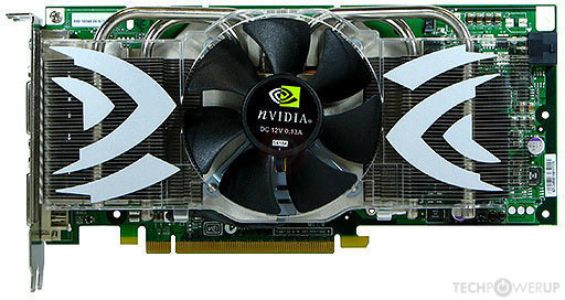
The GeForce 7900 GTX was a graphics card by NVIDIA, launched on March 9th, 2006. Built on the 90 nm process, and based on the G71 graphics processor, in its G71-U-N-A2 variant, the card supports DirectX 9.0c. Since GeForce 7900 GTX does not support DirectX 11 or DirectX 12, it might not be able to run all the latest games. The G71 graphics processor is an average sized chip with a die area of 196 mm² and 278 million transistors. It features 24 pixel shaders and 8 vertex shaders, 24 texture mapping units, and 16 ROPs. Due to the lack of unified shaders you will not be able to run recent games at all (which require unified shader/DX10+ support). NVIDIA has paired 512 MB GDDR3 memory with the GeForce 7900 GTX, which are connected using a 256-bit memory interface. The GPU is operating at a frequency of 650 MHz, memory is running at 800 MHz.
Being a dual-slot card, the NVIDIA GeForce 7900 GTX draws power from 1x 6-pin power connector, with power draw rated at 84 W maximum. Display outputs include: 2x DVI, 1x S-Video. GeForce 7900 GTX is connected to the rest of the system using a PCI-Express 1.0 x16 interface.
Being a dual-slot card, the NVIDIA GeForce 7900 GTX draws power from 1x 6-pin power connector, with power draw rated at 84 W maximum. Display outputs include: 2x DVI, 1x S-Video. GeForce 7900 GTX is connected to the rest of the system using a PCI-Express 1.0 x16 interface.
Graphics Processor
Graphics Card
- Release Date
- Mar 9th, 2006
- Generation
-
GeForce 7 PCIe
(7900)
- Predecessor
- GeForce 6 PCIe
- Successor
- GeForce 8
- Production
- End-of-life
- Bus Interface
- PCIe 1.0 x16
- Reviews
- 145 in our database
Clock Speeds
- GPU Clock
- 650 MHz
- Memory Clock
-
800 MHz
1600 Mbps effective
Memory
- Memory Size
- 512 MB
- Memory Type
- GDDR3
- Memory Bus
- 256 bit
- Bandwidth
- 51.20 GB/s
Render Config
- Pixel Shaders
- 24
- Vertex Shaders
- 8
- TMUs
- 24
- ROPs
- 16
Theoretical Performance
- Pixel Rate
- 10.40 GPixel/s
- Vertex Rate
- 1.300 GVertices/s
- Texture Rate
- 15.60 GTexel/s
Board Design
- Slot Width
- Dual-slot
- TDP
- 84 W
- Suggested PSU
- 250 W
- Outputs
- 2x DVI
1x S-Video
- Power Connectors
- 1x 6-pin
- Board Number
- P348
Graphics Features
- DirectX
- 9.0c (9_3)
- OpenGL
- 2.1
- OpenCL
- N/A
- Vulkan
- N/A
- Shader Model
- 3.0
G71 GPU Notes
| PureVideo HD: VP1 VDPAU: No Support |
Retail boards based on this design (4)
| Name | GPU Clock | Memory Clock | Other Changes |
|---|---|---|---|
| 650 MHz | 800 MHz | ||
| 690 MHz | 880 MHz | ||
| 675 MHz | 830 MHz | ||
| 650 MHz | 800 MHz |


Apr 19th, 2024 23:34 EDT
change timezone
Latest GPU Drivers
New Forum Posts
- I just succesfully baked DDR4 (76)
- GPU-Z reporting wrong ReBar info for RTX 20 series (4)
- I9 13890HX undervolting Suggestions (5)
- Official Board Game Discussion (4)
- Roccat Kone AIMO has developed a double left click, when I click it once. Any fix out there? (37)
- Cinebench crashed my PC. My Wi-Fi stopped working, and I keep getting a "Please wait" screen when I boot up my PC. (8)
- USB C to USB A hub (43)
- XFX RX580 stock Bios (8)
- Your PC ATM (34488)
- 2 questions about Oculus Quest 3 (0)
Popular Reviews
- Horizon Forbidden West Performance Benchmark Review - 30 GPUs Tested
- Fractal Design Terra Review
- Corsair 2000D Airflow Review
- Thermalright Phantom Spirit 120 EVO Review
- Minisforum EliteMini UM780 XTX (AMD Ryzen 7 7840HS) Review
- Creative Pebble X Plus Review
- FiiO KB3 HiFi Mechanical Keyboard Review - Integrated DAC/Amp!
- ASUS GeForce RTX 4090 STRIX OC Review
- NVIDIA GeForce RTX 4090 Founders Edition Review - Impressive Performance
- ASUS GeForce RTX 4090 Matrix Platinum Review - The RTX 4090 Ti
Controversial News Posts
- Sony PlayStation 5 Pro Specifications Confirmed, Console Arrives Before Holidays (111)
- NVIDIA Points Intel Raptor Lake CPU Users to Get Help from Intel Amid System Instability Issues (102)
- US Government Wants Nuclear Plants to Offload AI Data Center Expansion (98)
- AMD "Strix Halo" Zen 5 Mobile Processor Pictured: Chiplet-based, Uses 256-bit LPDDR5X (84)
- Windows 10 Security Updates to Cost $61 After 2025, $427 by 2028 (82)
- Developers of Outpost Infinity Siege Recommend Underclocking i9-13900K and i9-14900K for Stability on Machines with RTX 4090 (82)
- TechPowerUp Hiring: Reviewers Wanted for Motherboards, Laptops, Gaming Handhelds and Prebuilt Desktops (73)
- Intel Realizes the Only Way to Save x86 is to Democratize it, Reopens x86 IP Licensing (70)