Report an Error


NVIDIA GeForce 8800 GTS 320
- Graphics Processor
- G80
- Cores
- 96
- TMUs
- 24
- ROPs
- 20
- Memory Size
- 320 MB
- Memory Type
- GDDR3
- Bus Width
- 320 bit

GPU
Recommended Gaming Resolutions:
- 1366x768
- 1600x900
- 1920x1080
The GeForce 8800 GTS 320 was a performance-segment graphics card by NVIDIA, launched on February 12th, 2007. Built on the 90 nm process, and based on the G80 graphics processor, in its G80-100-K0-A2 variant, the card supports DirectX 11.1. Even though it supports DirectX 11, the feature level is only 10_0, which can be problematic with many DirectX 11 & DirectX 12 titles. The G80 graphics processor is a large chip with a die area of 484 mm² and 681 million transistors. Unlike the fully unlocked GeForce 8800 GTX, which uses the same GPU but has all 128 shaders enabled, NVIDIA has disabled some shading units on the GeForce 8800 GTS 320 to reach the product's target shader count. It features 96 shading units, 24 texture mapping units, and 20 ROPs. NVIDIA has paired 320 MB GDDR3 memory with the GeForce 8800 GTS 320, which are connected using a 320-bit memory interface. The GPU is operating at a frequency of 513 MHz, memory is running at 792 MHz.
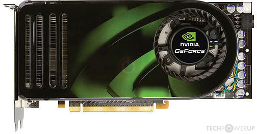
Being a dual-slot card, the NVIDIA GeForce 8800 GTS 320 draws power from 1x 6-pin power connector, with power draw rated at 143 W maximum. Display outputs include: 2x DVI, 1x S-Video. GeForce 8800 GTS 320 is connected to the rest of the system using a PCI-Express 1.0 x16 interface. The card measures 267 mm in length, and features a dual-slot cooling solution. Its price at launch was 269 US Dollars.
Being a dual-slot card, the NVIDIA GeForce 8800 GTS 320 draws power from 1x 6-pin power connector, with power draw rated at 143 W maximum. Display outputs include: 2x DVI, 1x S-Video. GeForce 8800 GTS 320 is connected to the rest of the system using a PCI-Express 1.0 x16 interface. The card measures 267 mm in length, and features a dual-slot cooling solution. Its price at launch was 269 US Dollars.
Graphics Processor
Graphics Card
- Release Date
- Feb 12th, 2007
- Generation
-
GeForce 8
(8800)
- Predecessor
- GeForce 7 PCIe
- Successor
- GeForce 9
- Production
- End-of-life
- Launch Price
- 269 USD
- Bus Interface
- PCIe 1.0 x16
- Reviews
- 403 in our database
Relative Performance
Based on TPU review data: "Performance Summary" at 1920x1080, 4K for 2080 Ti and faster.
Performance estimated based on architecture, shader count and clocks.
Clock Speeds
- GPU Clock
- 513 MHz
- Shader Clock
- 1188 MHz
- Memory Clock
-
792 MHz
1584 Mbps effective
Memory
- Memory Size
- 320 MB
- Memory Type
- GDDR3
- Memory Bus
- 320 bit
- Bandwidth
- 63.36 GB/s
Render Config
- Shading Units
- 96
- TMUs
- 24
- ROPs
- 20
- SM Count
- 12
- L2 Cache
- 80 KB
Theoretical Performance
- Pixel Rate
- 10.26 GPixel/s
- Texture Rate
- 24.62 GTexel/s
- FP32 (float)
- 228.1 GFLOPS
Board Design
- Slot Width
- Dual-slot
- Length
- 267 mm
10.5 inches
- TDP
- 143 W
- Suggested PSU
- 300 W
- Outputs
- 2x DVI
1x S-Video
- Power Connectors
- 1x 6-pin
- Board Number
- P356
Graphics Features
- DirectX
- 11.1 (10_0)
- OpenGL
- 3.3
- OpenCL
- 1.1 (1.0)
- Vulkan
- N/A
- CUDA
- 1.0
- Shader Model
- 4.0
G80 GPU Notes
| Each Streaming Multiprocessor(SM) in the chip architecture contains 8 SPs and 2 SFUs. Each SP can fulfill up to two single precision operations MAD per clock. Each SFU can fulfill up to four operations SF per clock (these units can also handle single-precision floating-point multiplications per clock). The approximate ratio of operations MAD to operations SF is equal 2:1. The theoretical SP + SFU performance in single-precision floating point operations [FLOPSsp + sfu, GFLOPS] of the graphics card with shader count [n] and shader frequency [f, GHz], is estimated by the following formula: FLOPSsp+sfu; f × n × 3. Alternative formula: FLOPSsp+sfu; f × m × ( 8 SPs * 2 (MAD) + 4 * 2 SFUs ). [m] - SM count. SP - Shader Processor (Unified Shader, CUDA Core) SFU - Special Function Unit SM - Streaming Multiprocessor MAD - ADD+MUL |
Retail boards based on this design (1)
| Name | GPU Clock | Memory Clock | Other Changes |
|---|---|---|---|
| 570 MHz | 900 MHz | 229 mm/9 inches |

Apr 24th, 2024 05:14 EDT
change timezone
Latest GPU Drivers
New Forum Posts
- What phone you use as your daily driver? And, a discussion of them. (1458)
- What's your latest tech purchase? (20329)
- Which new games will you be buying? (309)
- Official Board Game Discussion (15)
- The TPU UK Clubhouse (24775)
- Serious bug in PHP reported! (3)
- ThrottleStop 9.6 Voltage won't change (2)
- Sexy Mechanical Keyboard Thread (486)
- Is there a technical reason that Windows 11 doesn't have built into it battery charge limitation? (38)
- ROG Strix LC III 360 ARG AIO What should the pump speed be? (3)
Popular Reviews
- Fractal Design Terra Review
- Corsair 2000D Airflow Review
- Thermalright Phantom Spirit 120 EVO Review
- Minisforum EliteMini UM780 XTX (AMD Ryzen 7 7840HS) Review
- ASUS GeForce RTX 4090 STRIX OC Review
- NVIDIA GeForce RTX 4090 Founders Edition Review - Impressive Performance
- ASUS GeForce RTX 4090 Matrix Platinum Review - The RTX 4090 Ti
- MSI GeForce RTX 4090 Suprim X Review
- MSI GeForce RTX 4090 Gaming X Trio Review
- Gigabyte GeForce RTX 4090 Gaming OC Review
Controversial News Posts
- Sony PlayStation 5 Pro Specifications Confirmed, Console Arrives Before Holidays (116)
- NVIDIA Points Intel Raptor Lake CPU Users to Get Help from Intel Amid System Instability Issues (106)
- AMD "Strix Halo" Zen 5 Mobile Processor Pictured: Chiplet-based, Uses 256-bit LPDDR5X (101)
- US Government Wants Nuclear Plants to Offload AI Data Center Expansion (98)
- Windows 10 Security Updates to Cost $61 After 2025, $427 by 2028 (84)
- Developers of Outpost Infinity Siege Recommend Underclocking i9-13900K and i9-14900K for Stability on Machines with RTX 4090 (84)
- TechPowerUp Hiring: Reviewers Wanted for Motherboards, Laptops, Gaming Handhelds and Prebuilt Desktops (77)
- Intel Realizes the Only Way to Save x86 is to Democratize it, Reopens x86 IP Licensing (70)