Report an Error


NVIDIA GeForce 8400 GS Rev. 3
- Graphics Processor
- GT218S
- Cores
- 8
- TMUs
- 4
- ROPs
- 4
- Memory Size
- 512 MB
- Memory Type
- DDR2
- Bus Width
- 64 bit

GPU
Recommended Gaming Resolutions:
- 640x480
- 1280x720
- 1366x768
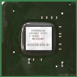
The GeForce 8400 GS Rev. 3 was a graphics card by NVIDIA, launched on July 12th, 2010. Built on the 40 nm process, and based on the GT218S graphics processor, in its 8400GS-225-B1 variant, the card supports DirectX 11.1. Even though it supports DirectX 11, the feature level is only 10_1, which can be problematic with many DirectX 11 & DirectX 12 titles. The GT218S graphics processor is a relatively small chip with a die area of only 57 mm² and 260 million transistors. Unlike the fully unlocked GeForce 8400 GS PCI Rev. 2, which uses the same GPU but has all 16 shaders enabled, NVIDIA has disabled some shading units on the GeForce 8400 GS Rev. 3 to reach the product's target shader count. It features 8 shading units, 4 texture mapping units, and 4 ROPs. NVIDIA has paired 512 MB DDR2 memory with the GeForce 8400 GS Rev. 3, which are connected using a 64-bit memory interface. The GPU is operating at a frequency of 520 MHz, memory is running at 400 MHz.
Being a single-slot card, the NVIDIA GeForce 8400 GS Rev. 3 does not require any additional power connector, its power draw is rated at 25 W maximum. Display outputs include: 1x DVI, 1x VGA, 1x S-Video. GeForce 8400 GS Rev. 3 is connected to the rest of the system using a PCI-Express 2.0 x16 interface. The card measures 170 mm in length, and features a single-slot cooling solution.
Being a single-slot card, the NVIDIA GeForce 8400 GS Rev. 3 does not require any additional power connector, its power draw is rated at 25 W maximum. Display outputs include: 1x DVI, 1x VGA, 1x S-Video. GeForce 8400 GS Rev. 3 is connected to the rest of the system using a PCI-Express 2.0 x16 interface. The card measures 170 mm in length, and features a single-slot cooling solution.
Graphics Processor
Graphics Card
- Release Date
- Jul 12th, 2010
- Generation
-
GeForce 8
(8400)
- Predecessor
- GeForce 7 PCIe
- Successor
- GeForce 9
- Production
- End-of-life
- Bus Interface
- PCIe 2.0 x16
- Reviews
- 10 in our database
Relative Performance
Based on TPU review data: "Performance Summary" at 1920x1080, 4K for 2080 Ti and faster.
Performance estimated based on architecture, shader count and clocks.
Clock Speeds
- GPU Clock
- 520 MHz
- Shader Clock
- 1230 MHz
- Memory Clock
-
400 MHz
800 Mbps effective
Memory
- Memory Size
- 512 MB
- Memory Type
- DDR2
- Memory Bus
- 64 bit
- Bandwidth
- 6.400 GB/s
Render Config
- Shading Units
- 8
- TMUs
- 4
- ROPs
- 4
- SM Count
- 1
- L2 Cache
- 32 KB
Theoretical Performance
- Pixel Rate
- 2.080 GPixel/s
- Texture Rate
- 2.080 GTexel/s
- FP32 (float)
- 19.68 GFLOPS
Board Design
- Slot Width
- Single-slot
- Length
- 170 mm
6.7 inches
- TDP
- 25 W
- Suggested PSU
- 200 W
- Outputs
- 1x DVI
1x VGA
1x S-Video
- Power Connectors
- None
- Board Number
- P691,
P872 SKU 0,
P872 SKU 2,
P873 SKU 0,
P874 SKU 5
Graphics Features
- DirectX
- 11.1 (10_1)
- OpenGL
- 3.3
- OpenCL
- 1.1
- Vulkan
- N/A
- CUDA
- 1.2
- Shader Model
- 4.1
GT218S GPU Notes
| PureVideo HD: VP4 VDPAU: Feature Set C |
Retail boards based on this design (1)
| Name | GPU Clock | Memory Clock | Other Changes |
|---|---|---|---|
| 520 MHz | 600 MHz | 1024 MB, DDR3, 165 mm/6.5 inches, 1x DVI 1x HDMI 1x VGA |

Apr 25th, 2024 09:32 EDT
change timezone
Latest GPU Drivers
New Forum Posts
- Asrock A770 Firmware (1)
- RTX 4070 vs RTX 4070 Ti power scaling (5)
- i7-12800HX Overheating Issues (2)
- (Anti) SFF fun house (354)
- What's your latest tech purchase? (20339)
- Alphacool CORE 1 CPU block - bulging with danger of splitting? (6)
- Bizarre Throttlestop issue (6)
- Core i5-6300U (17)
- Last game you purchased? (255)
- Drop fps (4)
Popular Reviews
- Fractal Design Terra Review
- Thermalright Phantom Spirit 120 EVO Review
- Corsair 2000D Airflow Review
- Minisforum EliteMini UM780 XTX (AMD Ryzen 7 7840HS) Review
- ASUS GeForce RTX 4090 STRIX OC Review
- NVIDIA GeForce RTX 4090 Founders Edition Review - Impressive Performance
- ASUS GeForce RTX 4090 Matrix Platinum Review - The RTX 4090 Ti
- MSI GeForce RTX 4090 Suprim X Review
- MSI GeForce RTX 4090 Gaming X Trio Review
- Gigabyte GeForce RTX 4090 Gaming OC Review
Controversial News Posts
- Sony PlayStation 5 Pro Specifications Confirmed, Console Arrives Before Holidays (116)
- NVIDIA Points Intel Raptor Lake CPU Users to Get Help from Intel Amid System Instability Issues (106)
- AMD "Strix Halo" Zen 5 Mobile Processor Pictured: Chiplet-based, Uses 256-bit LPDDR5X (101)
- US Government Wants Nuclear Plants to Offload AI Data Center Expansion (98)
- Windows 11 Now Officially Adware as Microsoft Embeds Ads in the Start Menu (88)
- Developers of Outpost Infinity Siege Recommend Underclocking i9-13900K and i9-14900K for Stability on Machines with RTX 4090 (85)
- Windows 10 Security Updates to Cost $61 After 2025, $427 by 2028 (84)
- AMD's RDNA 4 GPUs Could Stick with 18 Gbps GDDR6 Memory (82)