Report an Error


ATI Radeon HD 3850 X2
- Graphics Processor
- RV670 x2
- Cores
- 320 x2
- TMUs
- 16 x2
- ROPs
- 16 x2
- Memory Size
- 512 MB x2
- Memory Type
- GDDR3
- Bus Width
- 256 bit x2

GPU

I/O
Recommended Gaming Resolutions:
- 1366x768
- 1600x900
- 1920x1080
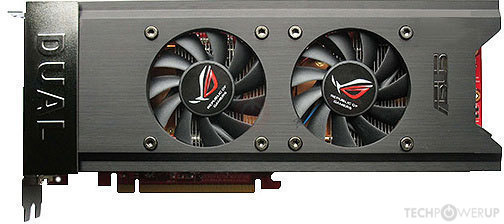
The Radeon HD 3850 X2 was a performance-segment graphics card by ATI, launched on April 4th, 2008. Built on the 55 nm process, and based on the RV670 graphics processor, in its RV670 PRO variant, the card supports DirectX 10.1. Since Radeon HD 3850 X2 does not support DirectX 11 or DirectX 12, it might not be able to run all the latest games. The RV670 graphics processor is an average sized chip with a die area of 192 mm² and 666 million transistors. Radeon HD 3850 X2 combines two graphics processors to increase performance. It features 320 shading units, 16 texture mapping units, and 16 ROPs, per GPU. ATI has paired 1,024 MB GDDR3 memory with the Radeon HD 3850 X2, which are connected using a 256-bit memory interface per GPU (each GPU manages 512 MB). The GPU is operating at a frequency of 669 MHz, memory is running at 828 MHz.
Being a dual-slot card, its power draw is rated at 140 W maximum. Display outputs include: 2x DVI, 1x S-Video. Radeon HD 3850 X2 is connected to the rest of the system using a PCI-Express 2.0 x16 interface. The card measures 267 mm in length, and features a dual-slot cooling solution. Its price at launch was 349 US Dollars.
Being a dual-slot card, its power draw is rated at 140 W maximum. Display outputs include: 2x DVI, 1x S-Video. Radeon HD 3850 X2 is connected to the rest of the system using a PCI-Express 2.0 x16 interface. The card measures 267 mm in length, and features a dual-slot cooling solution. Its price at launch was 349 US Dollars.
Graphics Processor
Graphics Card
- Release Date
- Apr 4th, 2008
- Generation
-
Radeon R600
(HD 3800)
- Predecessor
- Radeon R500 PCIe
- Successor
- Radeon R700
- Production
- End-of-life
- Launch Price
- 349 USD
- Bus Interface
- PCIe 2.0 x16
- Reviews
- 1 in our database
Relative Performance
Based on TPU review data: "Performance Summary" at 1920x1080, 4K for 2080 Ti and faster.
Performance estimated based on architecture, shader count and clocks.
Clock Speeds
- GPU Clock
- 669 MHz
- Memory Clock
-
828 MHz
1656 Mbps effective
Memory
- Memory Size
- 512 MB
- Memory Type
- GDDR3
- Memory Bus
- 256 bit
- Bandwidth
- 52.99 GB/s
Render Config
- Shading Units
- 320
- TMUs
- 16
- ROPs
- 16
- Compute Units
- 4
- L2 Cache
- 256 KB
Theoretical Performance
- Pixel Rate
- 10.70 GPixel/s
- Texture Rate
- 10.70 GTexel/s
- FP32 (float)
- 428.2 GFLOPS
- FP64 (double)
- 85.63 GFLOPS (1:5)
Board Design
- Slot Width
- Dual-slot
- Length
- 267 mm
10.5 inches
- TDP
- 140 W
- Suggested PSU
- 300 W
- Outputs
- 2x DVI
1x S-Video
Graphics Features
- DirectX
- 10.1 (10_1)
- OpenGL
-
3.3 (full)
4.0 (partial)
- OpenCL
- N/A
- Vulkan
- N/A
- Shader Model
- 4.1
RV670 GPU Notes
| Mobile Variant: M88 Codename: Boom Graphics/Compute: GFX3 Display Core Engine: 2.0 Unified Video Decoder: 1.0 RV670 Chip Numbers: RV670 XT (215-0708017) RV670 XTX ES (215-0708001) |
Retail boards based on this design (1)
| Name | GPU Clock | Memory Clock | Other Changes |
|---|---|---|---|
| 669 MHz | 828 MHz |

Apr 25th, 2024 11:01 EDT
change timezone
Latest GPU Drivers
New Forum Posts
- Meta Horizon OS (19)
- Rare GPUs / Unreleased GPUs (1876)
- i7-12800HX Overheating Issues (4)
- RTX 4070 vs RTX 4070 Ti power scaling (6)
- Low GPU FPS, gets fixed only after restart (15)
- Last game you purchased? (257)
- Alphacool CORE 1 CPU block - bulging with danger of splitting? (7)
- Ghost of Tsushima PC Port !!!! (14)
- How to check flatness of CPUs and coolers - INK and OPTICAL INTERFERENCE methods (109)
- (Anti) SFF fun house (355)
Popular Reviews
- Fractal Design Terra Review
- Thermalright Phantom Spirit 120 EVO Review
- Corsair 2000D Airflow Review
- Minisforum EliteMini UM780 XTX (AMD Ryzen 7 7840HS) Review
- ASUS GeForce RTX 4090 STRIX OC Review
- NVIDIA GeForce RTX 4090 Founders Edition Review - Impressive Performance
- ASUS GeForce RTX 4090 Matrix Platinum Review - The RTX 4090 Ti
- MSI GeForce RTX 4090 Suprim X Review
- MSI GeForce RTX 4090 Gaming X Trio Review
- Gigabyte GeForce RTX 4090 Gaming OC Review
Controversial News Posts
- Sony PlayStation 5 Pro Specifications Confirmed, Console Arrives Before Holidays (116)
- NVIDIA Points Intel Raptor Lake CPU Users to Get Help from Intel Amid System Instability Issues (106)
- AMD "Strix Halo" Zen 5 Mobile Processor Pictured: Chiplet-based, Uses 256-bit LPDDR5X (101)
- US Government Wants Nuclear Plants to Offload AI Data Center Expansion (98)
- Windows 11 Now Officially Adware as Microsoft Embeds Ads in the Start Menu (90)
- Developers of Outpost Infinity Siege Recommend Underclocking i9-13900K and i9-14900K for Stability on Machines with RTX 4090 (85)
- Windows 10 Security Updates to Cost $61 After 2025, $427 by 2028 (84)
- AMD's RDNA 4 GPUs Could Stick with 18 Gbps GDDR6 Memory (82)