Report an Error

ATI Radeon HD 4670
- Graphics Processor
- RV730
- Cores
- 320
- TMUs
- 32
- ROPs
- 8
- Memory Size
- 512 MB
- Memory Type
- GDDR3
- Bus Width
- 128 bit


GPU
Recommended Gaming Resolutions:
- 1280x720
- 1366x768
- 1600x900
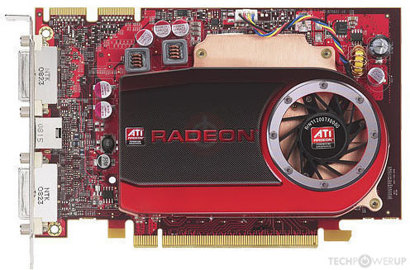
The Radeon HD 4670 was an entry-level graphics card by ATI, launched on September 10th, 2008. Built on the 55 nm process, and based on the RV730 graphics processor, in its RV730 XT variant, the card supports DirectX 10.1. Since Radeon HD 4670 does not support DirectX 11 or DirectX 12, it might not be able to run all the latest games. The RV730 graphics processor is an average sized chip with a die area of 146 mm² and 514 million transistors. It features 320 shading units, 32 texture mapping units, and 8 ROPs. ATI has paired 512 MB GDDR3 memory with the Radeon HD 4670, which are connected using a 128-bit memory interface. The GPU is operating at a frequency of 750 MHz, memory is running at 1000 MHz.
Being a single-slot card, the ATI Radeon HD 4670 does not require any additional power connector, its power draw is rated at 59 W maximum. Display outputs include: 2x DVI, 1x S-Video. Radeon HD 4670 is connected to the rest of the system using a PCI-Express 2.0 x16 interface. The card measures 193 mm in length, and features a single-slot cooling solution. Its price at launch was 67 US Dollars.
Being a single-slot card, the ATI Radeon HD 4670 does not require any additional power connector, its power draw is rated at 59 W maximum. Display outputs include: 2x DVI, 1x S-Video. Radeon HD 4670 is connected to the rest of the system using a PCI-Express 2.0 x16 interface. The card measures 193 mm in length, and features a single-slot cooling solution. Its price at launch was 67 US Dollars.
Graphics Processor
Graphics Card
- Release Date
- Sep 10th, 2008
- Generation
-
Radeon R700
(HD 4600)
- Predecessor
- Radeon R600
- Successor
- Evergreen
- Production
- End-of-life
- Launch Price
- 67 USD
- Bus Interface
- PCIe 2.0 x16
- Reviews
- 49 in our database
Relative Performance
Based on TPU review data: "Performance Summary" at 1920x1080, 4K for 2080 Ti and faster.
Clock Speeds
- GPU Clock
- 750 MHz
- Memory Clock
-
1000 MHz
2 Gbps effective
Memory
- Memory Size
- 512 MB
- Memory Type
- GDDR3
- Memory Bus
- 128 bit
- Bandwidth
- 32.00 GB/s
Render Config
- Shading Units
- 320
- TMUs
- 32
- ROPs
- 8
- Compute Units
- 4
- L1 Cache
- 16 KB (per CU)
- L2 Cache
- 128 KB
Theoretical Performance
- Pixel Rate
- 6.000 GPixel/s
- Texture Rate
- 24.00 GTexel/s
- FP32 (float)
- 480.0 GFLOPS
Board Design
- Slot Width
- Single-slot
- Length
- 193 mm
7.6 inches
- TDP
- 59 W
- Suggested PSU
- 250 W
- Outputs
- 2x DVI
1x S-Video
- Power Connectors
- None
- Board Number
- B666,
109-B70931-10
Graphics Features
- DirectX
- 10.1 (10_1)
- OpenGL
- 3.3
- OpenCL
- 1.1
- Vulkan
- N/A
- Shader Model
- 4.1
RV730 GPU Notes
| Mobile Variant: M96 Codename: Mario Graphics/Compute: GFX3 Display Core Engine: 3.2 Unified Video Decoder: 2.2 |
Retail boards based on this design (5)
| Name | GPU Clock | Memory Clock | Other Changes |
|---|---|---|---|
| 750 MHz | 800 MHz | 1024 MB, 203 mm/8 inches, Dual-slot | |
| 750 MHz | 800 MHz | 1024 MB, 203 mm/8 inches, Dual-slot, 1x DVI 1x HDMI 1x VGA | |
| 750 MHz | 1000 MHz | 1024 MB, 1x DVI 1x HDMI 1x VGA | |
| 750 MHz | 800 MHz | 1024 MB, 1x DVI 1x HDMI 1x VGA | |
| 750 MHz | 873 MHz | 1x DVI 1x HDMI 1x VGA |


Apr 23rd, 2024 02:04 EDT
change timezone
Latest GPU Drivers
New Forum Posts
- What are you playing? (20517)
- Which new games will you be buying? (293)
- EK seems to be having major issues (23)
- The TPU UK Clubhouse (24764)
- Why MS buying all of these Studios is bad for Gaming (12)
- Linus watercools (56)
- ASRock Deskmini Owner's Club (27)
- The best *budget* ATX PC case on the market? (20)
- TPU's Nostalgic Hardware Club (18459)
- AMD RX 7000 series GPU Owners' Club (1086)
Popular Reviews
- Horizon Forbidden West Performance Benchmark Review - 30 GPUs Tested
- Fractal Design Terra Review
- Corsair 2000D Airflow Review
- Thermalright Phantom Spirit 120 EVO Review
- Minisforum EliteMini UM780 XTX (AMD Ryzen 7 7840HS) Review
- ASUS GeForce RTX 4090 STRIX OC Review
- NVIDIA GeForce RTX 4090 Founders Edition Review - Impressive Performance
- ASUS GeForce RTX 4090 Matrix Platinum Review - The RTX 4090 Ti
- Creative Pebble X Plus Review
- MSI GeForce RTX 4090 Gaming X Trio Review
Controversial News Posts
- Sony PlayStation 5 Pro Specifications Confirmed, Console Arrives Before Holidays (115)
- NVIDIA Points Intel Raptor Lake CPU Users to Get Help from Intel Amid System Instability Issues (105)
- AMD "Strix Halo" Zen 5 Mobile Processor Pictured: Chiplet-based, Uses 256-bit LPDDR5X (101)
- US Government Wants Nuclear Plants to Offload AI Data Center Expansion (98)
- Windows 10 Security Updates to Cost $61 After 2025, $427 by 2028 (84)
- Developers of Outpost Infinity Siege Recommend Underclocking i9-13900K and i9-14900K for Stability on Machines with RTX 4090 (82)
- TechPowerUp Hiring: Reviewers Wanted for Motherboards, Laptops, Gaming Handhelds and Prebuilt Desktops (74)
- Intel Realizes the Only Way to Save x86 is to Democratize it, Reopens x86 IP Licensing (70)