Report an Error


AMD Radeon R9 295X2
- Graphics Processor
- Vesuvius x2
- Cores
- 2816 x2
- TMUs
- 176 x2
- ROPs
- 64 x2
- Memory Size
- 4 GB x2
- Memory Type
- GDDR5
- Bus Width
- 512 bit x2


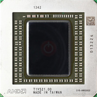
GPU
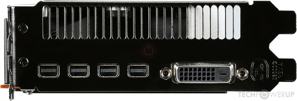
I/O
Top

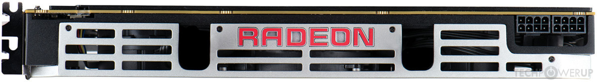
Back
Package

PCB Front
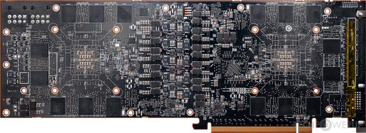
PCB Back
Recommended Gaming Resolutions:
- 1920x1080
- 2560x1440
- 3840x2160
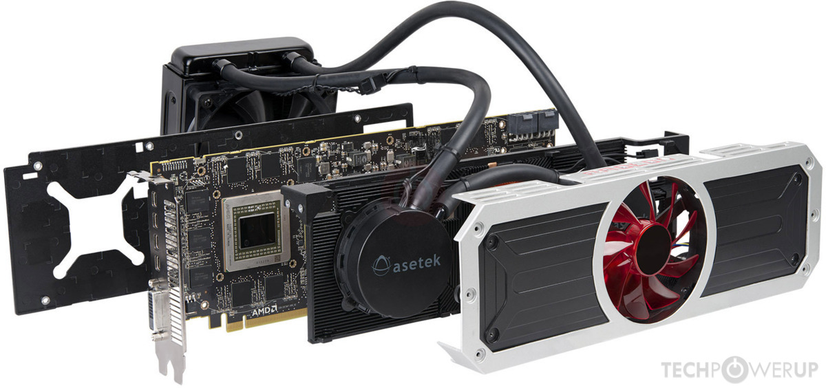
The Radeon R9 295X2 was an enthusiast-class graphics card by AMD, launched on April 29th, 2014. Built on the 28 nm process, and based on the Vesuvius graphics processor, in its Vesuvius XT variant, the card supports DirectX 12. This ensures that all modern games will run on Radeon R9 295X2. The Vesuvius graphics processor is a large chip with a die area of 438 mm² and 6,200 million transistors. Radeon R9 295X2 combines two graphics processors to increase performance. It features 2816 shading units, 176 texture mapping units, and 64 ROPs, per GPU. AMD has paired 8 GB GDDR5 memory with the Radeon R9 295X2, which are connected using a 512-bit memory interface per GPU (each GPU manages 4,096 MB). The GPU is operating at a frequency of 1018 MHz, memory is running at 1250 MHz (5 Gbps effective).
Being a dual-slot card, the AMD Radeon R9 295X2 draws power from 2x 8-pin power connectors, with power draw rated at 500 W maximum. Display outputs include: 1x DVI, 4x mini-DisplayPort 1.2. Radeon R9 295X2 is connected to the rest of the system using a PCI-Express 3.0 x16 interface. The card's dimensions are 307 mm x 114 mm x 42 mm, and it features a dual-slot cooling solution. Its price at launch was 1499 US Dollars.
Being a dual-slot card, the AMD Radeon R9 295X2 draws power from 2x 8-pin power connectors, with power draw rated at 500 W maximum. Display outputs include: 1x DVI, 4x mini-DisplayPort 1.2. Radeon R9 295X2 is connected to the rest of the system using a PCI-Express 3.0 x16 interface. The card's dimensions are 307 mm x 114 mm x 42 mm, and it features a dual-slot cooling solution. Its price at launch was 1499 US Dollars.
Graphics Processor
Graphics Card
- Release Date
- Apr 29th, 2014
- Generation
-
Volcanic Islands
(R9 200)
- Predecessor
- Sea Islands
- Successor
- Pirate Islands
- Production
- End-of-life
- Launch Price
- 1,499 USD
- Bus Interface
- PCIe 3.0 x16
- Reviews
- 33 in our database
Relative Performance
Based on TPU review data: "Performance Summary" at 1920x1080, 4K for 2080 Ti and faster.
Clock Speeds
- GPU Clock
- 1018 MHz
- Memory Clock
-
1250 MHz
5 Gbps effective
Memory
- Memory Size
- 4 GB
- Memory Type
- GDDR5
- Memory Bus
- 512 bit
- Bandwidth
- 320.0 GB/s
Render Config
- Shading Units
- 2816
- TMUs
- 176
- ROPs
- 64
- Compute Units
- 44
- L1 Cache
- 16 KB (per CU)
- L2 Cache
- 1024 KB
Theoretical Performance
- Pixel Rate
- 65.15 GPixel/s
- Texture Rate
- 179.2 GTexel/s
- FP32 (float)
- 5.733 TFLOPS
- FP64 (double)
- 716.7 GFLOPS (1:8)
Board Design
- Slot Width
- Dual-slot
- Length
- 307 mm
12.1 inches
- Width
- 114 mm
4.5 inches
- Height
- 42 mm
1.7 inches
- TDP
- 500 W
- Suggested PSU
- 900 W
- Outputs
- 1x DVI
4x mini-DisplayPort 1.2
- Power Connectors
- 2x 8-pin
- Board Number
- 109-C673A7-00D_02
Graphics Features
- DirectX
- 12 (12_0)
- OpenGL
- 4.6
- OpenCL
- 2.1
- Vulkan
- 1.2.170
- Shader Model
- 6.5
Vesuvius GPU Notes
| Generation: Volcanic Islands Desktop Variant: Hawaii / Grenada Graphics/Compute: GFX7 (gfx701) Display Core Engine: 8.5 Unified Video Decoder: 4.2 Video Compression Engine: 2.0 System DMA: 1.0.0 CLRX: GCN 1.1.0 |
Retail boards based on this design (13)
| Name | GPU Clock | Memory Clock | Other Changes |
|---|---|---|---|
| 1018 MHz | 1250 MHz | ||
| 1018 MHz | 1250 MHz | ||
| 1018 MHz | 1250 MHz | ||
| 1018 MHz | 1250 MHz | ||
| 1018 MHz | 1250 MHz | ||
| 1018 MHz | 1250 MHz | ||
| 1018 MHz | 1250 MHz | ||
| 1018 MHz | 1250 MHz | ||
| 1018 MHz | 1250 MHz | ||
| 1030 MHz | 1300 MHz | ||
| 1018 MHz | 1250 MHz | Single-slot | |
| 1018 MHz | 1250 MHz | ||
| 1018 MHz | 1250 MHz |


Apr 19th, 2024 03:58 EDT
change timezone
Latest GPU Drivers
New Forum Posts
- First computer build for my son (2)
- Linus watercools (18)
- Unlocked Realtek HD Audio Drivers for Windows 11 (Dolby Digital Live/DTS Interactive) (154)
- Ghetto Mods (4318)
- Identify my GPU - RX 570 8GB (or what?) (3)
- FINAL FANTASY XIV: Dawntrail Official Benchmark (58)
- What's your latest tech purchase? (20283)
- Should the CDPR make the Fallout 5 instead? (23)
- Will a RTX 4070 TI super bottleneck a Ryzen 9 7950X3D? (36)
- DDR5 RAM Speeds and the future (45)
Popular Reviews
- Horizon Forbidden West Performance Benchmark Review - 30 GPUs Tested
- PowerColor Radeon RX 7900 GRE Hellhound Review
- Fractal Design Terra Review
- Corsair 2000D Airflow Review
- Minisforum EliteMini UM780 XTX (AMD Ryzen 7 7840HS) Review
- Thermalright Phantom Spirit 120 EVO Review
- Creative Pebble X Plus Review
- FiiO KB3 HiFi Mechanical Keyboard Review - Integrated DAC/Amp!
- ASUS GeForce RTX 4090 STRIX OC Review
- NVIDIA GeForce RTX 4090 Founders Edition Review - Impressive Performance
Controversial News Posts
- Sony PlayStation 5 Pro Specifications Confirmed, Console Arrives Before Holidays (110)
- NVIDIA Points Intel Raptor Lake CPU Users to Get Help from Intel Amid System Instability Issues (102)
- US Government Wants Nuclear Plants to Offload AI Data Center Expansion (98)
- Windows 10 Security Updates to Cost $61 After 2025, $427 by 2028 (82)
- Developers of Outpost Infinity Siege Recommend Underclocking i9-13900K and i9-14900K for Stability on Machines with RTX 4090 (82)
- TechPowerUp Hiring: Reviewers Wanted for Motherboards, Laptops, Gaming Handhelds and Prebuilt Desktops (71)
- Intel Realizes the Only Way to Save x86 is to Democratize it, Reopens x86 IP Licensing (70)
- AMD Zen 5 Execution Engine Leaked, Features True 512-bit FPU (63)