Report an Error


ATI Radeon HD 5970
- Graphics Processor
- Hemlock x2
- Cores
- 1600 x2
- TMUs
- 80 x2
- ROPs
- 32 x2
- Memory Size
- 1024 MB x2
- Memory Type
- GDDR5
- Bus Width
- 256 bit x2


GPU
I/O

Bottom

Rear

Back
PCB Front

PCB Back
Recommended Gaming Resolutions:
- 1600x900
- 1920x1080
- 2560x1440
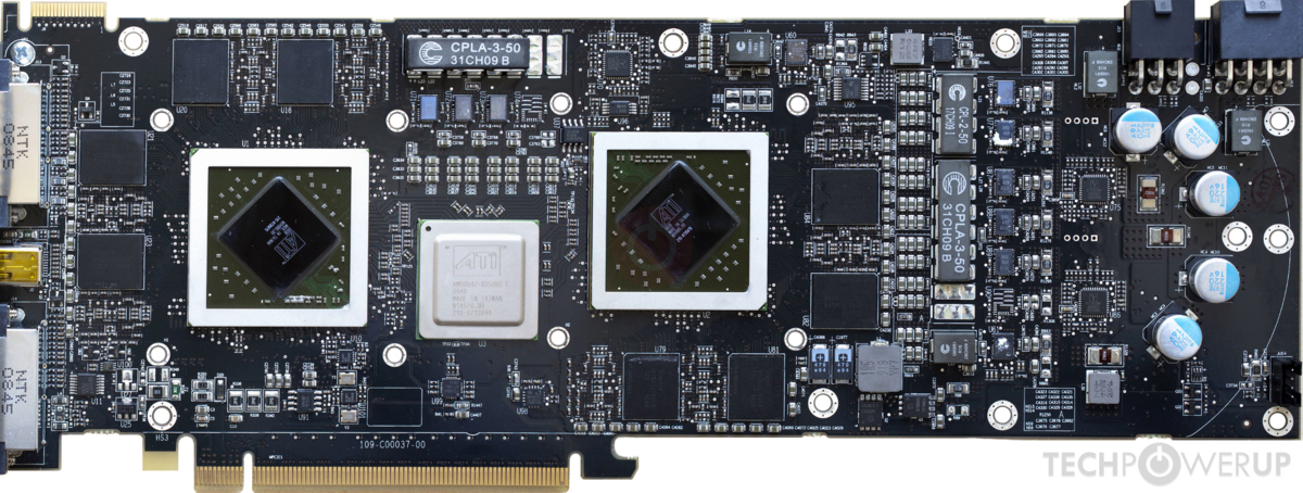
The Radeon HD 5970 was an enthusiast-class graphics card by ATI, launched on November 18th, 2009. Built on the 40 nm process, and based on the Hemlock graphics processor, in its Hemlock XT variant, the card supports DirectX 11.2. The Hemlock graphics processor is a large chip with a die area of 334 mm² and 2,154 million transistors. Radeon HD 5970 combines two graphics processors to increase performance. It features 1600 shading units, 80 texture mapping units, and 32 ROPs, per GPU. ATI has paired 2,048 MB GDDR5 memory with the Radeon HD 5970, which are connected using a 256-bit memory interface per GPU (each GPU manages 1,024 MB). The GPU is operating at a frequency of 725 MHz, memory is running at 1000 MHz (4 Gbps effective).
Being a dual-slot card, the ATI Radeon HD 5970 draws power from 1x 6-pin + 1x 8-pin power connector, with power draw rated at 294 W maximum. Display outputs include: 2x DVI, 1x mini-DisplayPort 1.1. Radeon HD 5970 is connected to the rest of the system using a PCI-Express 2.0 x16 interface. The card's dimensions are 311 mm x 111 mm x 37 mm, and it features a dual-slot cooling solution. Its price at launch was 699 US Dollars.
Being a dual-slot card, the ATI Radeon HD 5970 draws power from 1x 6-pin + 1x 8-pin power connector, with power draw rated at 294 W maximum. Display outputs include: 2x DVI, 1x mini-DisplayPort 1.1. Radeon HD 5970 is connected to the rest of the system using a PCI-Express 2.0 x16 interface. The card's dimensions are 311 mm x 111 mm x 37 mm, and it features a dual-slot cooling solution. Its price at launch was 699 US Dollars.
Graphics Processor
- GPU Name
- Hemlock
- GPU Variant
-
Hemlock XT
(215-0735075)
- Architecture
- TeraScale 2
- Foundry
- TSMC
- Process Size
- 40 nm
- Transistors
- 2,154 million
- Density
- 6.4M / mm²
- Die Size
- 334 mm²
Graphics Card
- Release Date
- Nov 18th, 2009
- Generation
-
Evergreen
(HD 5900)
- Predecessor
- Radeon R700
- Successor
- Northern Islands
- Production
- End-of-life
- Launch Price
- 699 USD
- Bus Interface
- PCIe 2.0 x16
- Reviews
- 74 in our database
Relative Performance
Based on TPU review data: "Performance Summary" at 1920x1080, 4K for 2080 Ti and faster.
Clock Speeds
- GPU Clock
- 725 MHz
- Memory Clock
-
1000 MHz
4 Gbps effective
Memory
- Memory Size
- 1024 MB
- Memory Type
- GDDR5
- Memory Bus
- 256 bit
- Bandwidth
- 128.0 GB/s
Render Config
- Shading Units
- 1600
- TMUs
- 80
- ROPs
- 32
- Compute Units
- 20
- L1 Cache
- 8 KB (per CU)
- L2 Cache
- 512 KB
Theoretical Performance
- Pixel Rate
- 23.20 GPixel/s
- Texture Rate
- 58.00 GTexel/s
- FP32 (float)
- 2.320 TFLOPS
- FP64 (double)
- 464.0 GFLOPS (1:5)
Board Design
- Slot Width
- Dual-slot
- Length
- 311 mm
12.2 inches
- Width
- 111 mm
4.4 inches
- Height
- 37 mm
1.5 inches
- TDP
- 294 W
- Suggested PSU
- 600 W
- Outputs
- 2x DVI
1x mini-DisplayPort 1.1
- Power Connectors
- 1x 6-pin + 1x 8-pin
- Board Number
- 109-C00037-00
Graphics Features
- DirectX
- 11.2 (11_0)
- OpenGL
- 4.4
- OpenCL
- 1.2
- Vulkan
- N/A
- Shader Model
- 5.0
Hemlock GPU Notes
| Generation: Evergreen Desktop Variant: Cypress Mobile Variant: Lexington Graphics/Compute: GFX4 Display Core Engine: 4.0 Unified Video Decoder: 2.3 |
Retail boards based on this design (10)
| Name | GPU Clock | Memory Clock | Other Changes |
|---|---|---|---|
| 850 MHz | 1200 MHz | 2 GB, 279 mm/11 inches, 2x DVI 1x HDMI 1x DisplayPort | |
| 725 MHz | 1000 MHz | ||
| 725 MHz | 1000 MHz | ||
| 750 MHz | 1050 MHz | ||
| 725 MHz | 1000 MHz | ||
| 850 MHz | 1200 MHz | 2 GB, 310 mm/12.2 inches | |
| 735 MHz | 1010 MHz | ||
| 900 MHz | 1200 MHz | 2 GB, 310 mm/12.2 inches | |
| 725 MHz | 1000 MHz | ||
| 850 MHz | 1200 MHz | 2 GB, 6x mini-DisplayPort |


Apr 25th, 2024 12:40 EDT
change timezone
Latest GPU Drivers
New Forum Posts
- Meta Horizon OS (20)
- WCG Daily Numbers (12497)
- Share your AIDA 64 cache and memory benchmark here (2917)
- Best SSD for system drive (76)
- Ghetto Mods (4319)
- How to check flatness of CPUs and coolers - INK and OPTICAL INTERFERENCE methods (110)
- Have you got pie today? (16317)
- Milestones (13874)
- TPU's Rosetta Milestones and Daily Pie Thread (1859)
- ThrottleStop 9.6 Voltage won't change (4)
Popular Reviews
- Fractal Design Terra Review
- Thermalright Phantom Spirit 120 EVO Review
- Corsair 2000D Airflow Review
- Minisforum EliteMini UM780 XTX (AMD Ryzen 7 7840HS) Review
- ASUS GeForce RTX 4090 STRIX OC Review
- NVIDIA GeForce RTX 4090 Founders Edition Review - Impressive Performance
- ASUS GeForce RTX 4090 Matrix Platinum Review - The RTX 4090 Ti
- MSI GeForce RTX 4090 Suprim X Review
- MSI GeForce RTX 4090 Gaming X Trio Review
- Gigabyte GeForce RTX 4090 Gaming OC Review
Controversial News Posts
- Sony PlayStation 5 Pro Specifications Confirmed, Console Arrives Before Holidays (116)
- NVIDIA Points Intel Raptor Lake CPU Users to Get Help from Intel Amid System Instability Issues (106)
- AMD "Strix Halo" Zen 5 Mobile Processor Pictured: Chiplet-based, Uses 256-bit LPDDR5X (101)
- US Government Wants Nuclear Plants to Offload AI Data Center Expansion (98)
- Windows 11 Now Officially Adware as Microsoft Embeds Ads in the Start Menu (94)
- AMD's RDNA 4 GPUs Could Stick with 18 Gbps GDDR6 Memory (85)
- Developers of Outpost Infinity Siege Recommend Underclocking i9-13900K and i9-14900K for Stability on Machines with RTX 4090 (85)
- Windows 10 Security Updates to Cost $61 After 2025, $427 by 2028 (84)