Report an Error


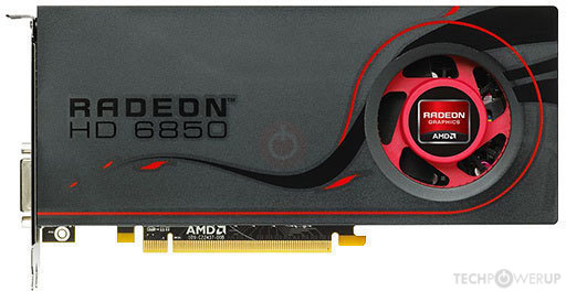
AMD Radeon HD 6850
- Graphics Processor
- Barts
- Cores
- 960
- TMUs
- 48
- ROPs
- 32
- Memory Size
- 1024 MB
- Memory Type
- GDDR5
- Bus Width
- 256 bit

GPU

I/O

Top

Bottom

Rear

Back
Recommended Gaming Resolutions:
- 1600x900
- 1920x1080
- 2560x1440
The Radeon HD 6850 was a mid-range graphics card by AMD, launched on October 21st, 2010. Built on the 40 nm process, and based on the Barts graphics processor, in its Barts PRO variant, the card supports DirectX 11.2. The Barts graphics processor is an average sized chip with a die area of 255 mm² and 1,700 million transistors. Unlike the fully unlocked Radeon HD 6870, which uses the same GPU but has all 1120 shaders enabled, AMD has disabled some shading units on the Radeon HD 6850 to reach the product's target shader count. It features 960 shading units, 48 texture mapping units, and 32 ROPs. AMD has paired 1,024 MB GDDR5 memory with the Radeon HD 6850, which are connected using a 256-bit memory interface. The GPU is operating at a frequency of 775 MHz, memory is running at 1000 MHz (4 Gbps effective).
Being a dual-slot card, the AMD Radeon HD 6850 draws power from 1x 6-pin power connector, with power draw rated at 127 W maximum. Display outputs include: 2x DVI, 1x HDMI 1.3a, 2x mini-DisplayPort 1.1. Radeon HD 6850 is connected to the rest of the system using a PCI-Express 2.0 x16 interface. The card measures 198 mm in length, and features a dual-slot cooling solution. Its price at launch was 179 US Dollars.
Being a dual-slot card, the AMD Radeon HD 6850 draws power from 1x 6-pin power connector, with power draw rated at 127 W maximum. Display outputs include: 2x DVI, 1x HDMI 1.3a, 2x mini-DisplayPort 1.1. Radeon HD 6850 is connected to the rest of the system using a PCI-Express 2.0 x16 interface. The card measures 198 mm in length, and features a dual-slot cooling solution. Its price at launch was 179 US Dollars.
Graphics Processor
- GPU Name
- Barts
- GPU Variant
-
Barts PRO
(215-0798006)
- Architecture
- TeraScale 2
- Foundry
- TSMC
- Process Size
- 40 nm
- Transistors
- 1,700 million
- Density
- 6.7M / mm²
- Die Size
- 255 mm²
- Chip Package
- HFCBGA-1737
Graphics Card
- Release Date
- Oct 21st, 2010
- Generation
-
Northern Islands
(HD 6800)
- Predecessor
- Evergreen
- Successor
- Southern Islands
- Production
- End-of-life
- Launch Price
- 179 USD
- Bus Interface
- PCIe 2.0 x16
- Reviews
- 105 in our database
Relative Performance
Based on TPU review data: "Performance Summary" at 1920x1080, 4K for 2080 Ti and faster.
Clock Speeds
- GPU Clock
- 775 MHz
- Memory Clock
-
1000 MHz
4 Gbps effective
Memory
- Memory Size
- 1024 MB
- Memory Type
- GDDR5
- Memory Bus
- 256 bit
- Bandwidth
- 128.0 GB/s
Render Config
- Shading Units
- 960
- TMUs
- 48
- ROPs
- 32
- Compute Units
- 12
- L1 Cache
- 8 KB (per CU)
- L2 Cache
- 512 KB
Theoretical Performance
- Pixel Rate
- 24.80 GPixel/s
- Texture Rate
- 37.20 GTexel/s
- FP32 (float)
- 1,488 GFLOPS
Board Design
- Slot Width
- Dual-slot
- Length
- 198 mm
7.8 inches
- TDP
- 127 W
- Suggested PSU
- 300 W
- Outputs
- 2x DVI
1x HDMI 1.3a
2x mini-DisplayPort 1.1
- Power Connectors
- 1x 6-pin
- Board Number
- 109-C22301-00B
Graphics Features
- DirectX
- 11.2 (11_0)
- OpenGL
- 4.4
- OpenCL
- 1.2
- Vulkan
- N/A
- Shader Model
- 5.0
Barts GPU Notes
| Generation: Northern Islands Mobile Variant: Blackcomb Codename: Victoria Graphics/Compute: GFX4 Display Core Engine: 5.0 Unified Video Decoder: 3.1 |
Retail boards based on this design (20)
| Name | GPU Clock | Memory Clock | Other Changes |
|---|---|---|---|
| 790 MHz | 1000 MHz | 260 mm/10.2 inches, 2x DVI 1x HDMI 1x DisplayPort | |
| 790 MHz | 1000 MHz | 260 mm/10.2 inches, 2x DVI 1x HDMI 1x DisplayPort | |
| 775 MHz | 1000 MHz | 235 mm/9.3 inches, 2x DVI 1x HDMI 1x DisplayPort | |
| 775 MHz | 1000 MHz | 235 mm/9.3 inches, 2x DVI 1x HDMI 1x DisplayPort | |
| 775 MHz | 1000 MHz | 235 mm/9.3 inches, 2x DVI 1x HDMI 1x DisplayPort | |
| 820 MHz | 1100 MHz | 235 mm/9.3 inches, 2x DVI 1x HDMI 1x DisplayPort | |
| 800 MHz | 1000 MHz | 226 mm/8.9 inches, 2x DVI 1x HDMI 1x DisplayPort | |
| 820 MHz | 1100 MHz | 226 mm/8.9 inches, 2x DVI 1x HDMI 1x DisplayPort | |
| 860 MHz | 1100 MHz | 217 mm/8.5 inches, 2x DVI 1x HDMI 1x DisplayPort | |
| 820 MHz | 1100 MHz | 241 mm/9.5 inches | |
| 800 MHz | 1100 MHz | 238 mm/9.4 inches | |
| 775 MHz | 1000 MHz | 2x DVI 1x HDMI 1x DisplayPort | |
| 800 MHz | 1050 MHz | ||
| 775 MHz | 1000 MHz | 235 mm/9.3 inches | |
| 775 MHz | 1000 MHz | 220 mm/8.7 inches | |
| 820 MHz | 1100 MHz | 235 mm/9.3 inches, 2x DVI 1x HDMI 1x DisplayPort | |
| 820 MHz | 1100 MHz | 235 mm/9.3 inches, 2x DVI 1x HDMI 1x DisplayPort | |
| 775 MHz | 1000 MHz | 1x DVI 1x HDMI 1x VGA | |
| 800 MHz | 1050 MHz | 235 mm/9.3 inches, 2x DVI 1x HDMI 1x DisplayPort | |
| 800 MHz | 1050 MHz | 235 mm/9.3 inches, 2x DVI 1x HDMI 1x DisplayPort |


Apr 25th, 2024 12:19 EDT
change timezone
Latest GPU Drivers
New Forum Posts
- Share your AIDA 64 cache and memory benchmark here (2917)
- Best SSD for system drive (76)
- Ghetto Mods (4319)
- How to check flatness of CPUs and coolers - INK and OPTICAL INTERFERENCE methods (110)
- Have you got pie today? (16317)
- Milestones (13874)
- WCG Daily Numbers (12496)
- TPU's Rosetta Milestones and Daily Pie Thread (1859)
- ThrottleStop 9.6 Voltage won't change (4)
- Folding Pie and Milestones!! (9008)
Popular Reviews
- Fractal Design Terra Review
- Thermalright Phantom Spirit 120 EVO Review
- Corsair 2000D Airflow Review
- Minisforum EliteMini UM780 XTX (AMD Ryzen 7 7840HS) Review
- ASUS GeForce RTX 4090 STRIX OC Review
- NVIDIA GeForce RTX 4090 Founders Edition Review - Impressive Performance
- ASUS GeForce RTX 4090 Matrix Platinum Review - The RTX 4090 Ti
- MSI GeForce RTX 4090 Suprim X Review
- MSI GeForce RTX 4090 Gaming X Trio Review
- Gigabyte GeForce RTX 4090 Gaming OC Review
Controversial News Posts
- Sony PlayStation 5 Pro Specifications Confirmed, Console Arrives Before Holidays (116)
- NVIDIA Points Intel Raptor Lake CPU Users to Get Help from Intel Amid System Instability Issues (106)
- AMD "Strix Halo" Zen 5 Mobile Processor Pictured: Chiplet-based, Uses 256-bit LPDDR5X (101)
- US Government Wants Nuclear Plants to Offload AI Data Center Expansion (98)
- Windows 11 Now Officially Adware as Microsoft Embeds Ads in the Start Menu (94)
- AMD's RDNA 4 GPUs Could Stick with 18 Gbps GDDR6 Memory (85)
- Developers of Outpost Infinity Siege Recommend Underclocking i9-13900K and i9-14900K for Stability on Machines with RTX 4090 (85)
- Windows 10 Security Updates to Cost $61 After 2025, $427 by 2028 (84)