Report an Error


AMD Radeon HD 6950M
- Graphics Processor
- Blackcomb
- Cores
- 960
- TMUs
- 48
- ROPs
- 32
- Memory Size
- 1024 MB
- Memory Type
- GDDR5
- Bus Width
- 256 bit

GPU
Recommended Gaming Resolutions:
- 1600x900
- 1920x1080
- 2560x1440
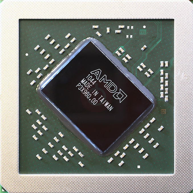
The Radeon HD 6950M was a mobile graphics chip by AMD, launched on January 4th, 2011. Built on the 40 nm process, and based on the Blackcomb graphics processor, in its Blackcomb PRO variant, the chip supports DirectX 11.2. The Blackcomb graphics processor is an average sized chip with a die area of 212 mm² and 1,700 million transistors. Unlike the fully unlocked Radeon HD 6990M, which uses the same GPU but has all 1120 shaders enabled, AMD has disabled some shading units on the Radeon HD 6950M to reach the product's target shader count. It features 960 shading units, 48 texture mapping units, and 32 ROPs. AMD has paired 1,024 MB GDDR5 memory with the Radeon HD 6950M, which are connected using a 256-bit memory interface. The GPU is operating at a frequency of 580 MHz, memory is running at 900 MHz (3.6 Gbps effective).
Being a mxm module card, its power draw is rated at 50 W maximum. This device has no display connectivity, as it is not designed to have monitors connected to it. Rather it is intended for use in laptop/notebooks and will use the output of the host mobile device.
Being a mxm module card, its power draw is rated at 50 W maximum. This device has no display connectivity, as it is not designed to have monitors connected to it. Rather it is intended for use in laptop/notebooks and will use the output of the host mobile device.
Graphics Processor
- GPU Name
- Blackcomb
- GPU Variant
-
Blackcomb PRO
(216-0811004)
- Architecture
- TeraScale 2
- Foundry
- TSMC
- Process Size
- 40 nm
- Transistors
- 1,700 million
- Density
- 8.0M / mm²
- Die Size
- 212 mm²
- Chip Package
- HFCBGA-1737
Mobile Graphics
Relative Performance
Based on TPU review data: "Performance Summary" at 1920x1080, 4K for 2080 Ti and faster.
Performance estimated based on architecture, shader count and clocks.
Clock Speeds
- GPU Clock
- 580 MHz
- Memory Clock
-
900 MHz
3.6 Gbps effective
Memory
- Memory Size
- 1024 MB
- Memory Type
- GDDR5
- Memory Bus
- 256 bit
- Bandwidth
- 115.2 GB/s
Render Config
- Shading Units
- 960
- TMUs
- 48
- ROPs
- 32
- Compute Units
- 12
- L1 Cache
- 8 KB (per CU)
- L2 Cache
- 512 KB
Theoretical Performance
- Pixel Rate
- 18.56 GPixel/s
- Texture Rate
- 27.84 GTexel/s
- FP32 (float)
- 1,114 GFLOPS
Board Design
- Slot Width
- MXM Module
- TDP
- 50 W
- Outputs
- Portable Device Dependent
Graphics Features
- DirectX
- 11.2 (11_0)
- OpenGL
- 4.4
- OpenCL
- 1.2
- Vulkan
- N/A
- Shader Model
- 5.0
Blackcomb GPU Notes
| Generation: Northern Islands Desktop Variant: Barts Graphics/Compute: GFX4 Display Core Engine: 5.0 Unified Video Decoder: 3.1 |
Devices based on this design (1)
| Name | GPU Clock | Memory Clock | Other Changes |
|---|---|---|---|
| 580 MHz | 900 MHz | 2 GB |

Apr 18th, 2024 06:03 EDT
change timezone
Latest GPU Drivers
New Forum Posts
- Realtek Modded Audio Driver for Windows 10/11 - Only for HDAUDIO (5677)
- Which air cooler for a ryzen 9 5900x (155)
- Your PC ATM (34484)
- Unlocked Realtek HD Audio Drivers for Windows 11 (Dolby Digital Live/DTS Interactive) (151)
- Will a RTX 4070 TI super bottleneck a Ryzen 9 7950X3D? (31)
- Issue of the RTX 4050's L2 Cache in the Techpowerup GPU Database (0)
- Post your JetStream 2 speeds! (140)
- The TPU UK Clubhouse (24725)
- Sold my a working PSU that I have been using, but buyer says it sparked at the outlet when he plugged it in and asking for a possible refund (9)
- Gigabyte gpu model differences? (30)
Popular Reviews
- Horizon Forbidden West Performance Benchmark Review - 30 GPUs Tested
- PowerColor Radeon RX 7900 GRE Hellhound Review
- ASUS GeForce RTX 4090 Matrix Platinum Review - The RTX 4090 Ti
- Fractal Design Terra Review
- Corsair 2000D Airflow Review
- Minisforum EliteMini UM780 XTX (AMD Ryzen 7 7840HS) Review
- Creative Pebble X Plus Review
- FiiO KB3 HiFi Mechanical Keyboard Review - Integrated DAC/Amp!
- ASUS GeForce RTX 4090 STRIX OC Review
- NVIDIA GeForce RTX 4090 Founders Edition Review - Impressive Performance
Controversial News Posts
- Sony PlayStation 5 Pro Specifications Confirmed, Console Arrives Before Holidays (106)
- NVIDIA Points Intel Raptor Lake CPU Users to Get Help from Intel Amid System Instability Issues (102)
- US Government Wants Nuclear Plants to Offload AI Data Center Expansion (98)
- Windows 10 Security Updates to Cost $61 After 2025, $427 by 2028 (82)
- Developers of Outpost Infinity Siege Recommend Underclocking i9-13900K and i9-14900K for Stability on Machines with RTX 4090 (82)
- TechPowerUp Hiring: Reviewers Wanted for Motherboards, Laptops, Gaming Handhelds and Prebuilt Desktops (71)
- Intel Realizes the Only Way to Save x86 is to Democratize it, Reopens x86 IP Licensing (70)
- AMD Zen 5 Execution Engine Leaked, Features True 512-bit FPU (63)