Report an Error


NVIDIA GeForce GTS 450 Rev. 2
- Graphics Processor
- GF116
- Cores
- 192
- TMUs
- 32
- ROPs
- 16
- Memory Size
- 1024 MB
- Memory Type
- GDDR5
- Bus Width
- 128 bit

GPU
Recommended Gaming Resolutions:
- 1366x768
- 1600x900
- 1920x1080
The GeForce GTS 450 Rev. 2 was a graphics card by NVIDIA, launched on March 15th, 2011. Built on the 40 nm process, and based on the GF116 graphics processor, in its GF116-200-KA-A1 variant, the card supports DirectX 12. Even though it supports DirectX 12, the feature level is only 11_0, which can be problematic with newer DirectX 12 titles. The GF116 graphics processor is an average sized chip with a die area of 238 mm² and 1,170 million transistors. It features 192 shading units, 32 texture mapping units, and 16 ROPs. NVIDIA has paired 1,024 MB GDDR5 memory with the GeForce GTS 450 Rev. 2, which are connected using a 128-bit memory interface. The GPU is operating at a frequency of 783 MHz, memory is running at 902 MHz (3.6 Gbps effective).
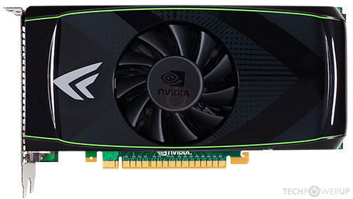
Being a dual-slot card, the NVIDIA GeForce GTS 450 Rev. 2 draws power from 1x 6-pin power connector, with power draw rated at 106 W maximum. Display outputs include: 2x DVI, 1x mini-HDMI 1.3a. GeForce GTS 450 Rev. 2 is connected to the rest of the system using a PCI-Express 2.0 x16 interface. The card measures 210 mm in length, and features a dual-slot cooling solution.
Being a dual-slot card, the NVIDIA GeForce GTS 450 Rev. 2 draws power from 1x 6-pin power connector, with power draw rated at 106 W maximum. Display outputs include: 2x DVI, 1x mini-HDMI 1.3a. GeForce GTS 450 Rev. 2 is connected to the rest of the system using a PCI-Express 2.0 x16 interface. The card measures 210 mm in length, and features a dual-slot cooling solution.
Graphics Processor
Graphics Card
- Release Date
- Mar 15th, 2011
- Generation
- GeForce 400
- Predecessor
- GeForce 200
- Successor
- GeForce 500
- Production
- End-of-life
- Bus Interface
- PCIe 2.0 x16
- Reviews
- 80 in our database
Relative Performance
Based on TPU review data: "Performance Summary" at 1920x1080, 4K for 2080 Ti and faster.
Performance estimated based on architecture, shader count and clocks.
Clock Speeds
- GPU Clock
- 783 MHz
- Shader Clock
- 1566 MHz
- Memory Clock
-
902 MHz
3.6 Gbps effective
Memory
- Memory Size
- 1024 MB
- Memory Type
- GDDR5
- Memory Bus
- 128 bit
- Bandwidth
- 57.73 GB/s
Render Config
- Shading Units
- 192
- TMUs
- 32
- ROPs
- 16
- SM Count
- 4
- L1 Cache
- 64 KB (per SM)
- L2 Cache
- 256 KB
Theoretical Performance
- Pixel Rate
- 6.264 GPixel/s
- Texture Rate
- 25.06 GTexel/s
- FP32 (float)
- 601.3 GFLOPS
- FP64 (double)
- 50.11 GFLOPS (1:12)
Board Design
- Slot Width
- Dual-slot
- Length
- 210 mm
8.3 inches
- TDP
- 106 W
- Suggested PSU
- 300 W
- Outputs
- 2x DVI
1x mini-HDMI 1.3a
- Power Connectors
- 1x 6-pin
- Board Number
- P1060 SKU 50,
P1062 SKU 1,
P1062 SKU 16,
P1428 SKU 10
Graphics Features
- DirectX
- 12 (11_0)
- OpenGL
- 4.6
- OpenCL
- 1.1
- Vulkan
- N/A
- CUDA
- 2.1
- Shader Model
- 5.1
GF116 GPU Notes
| PureVideo HD: VP4 VDPAU: Feature Set C |
Retail boards based on this design (2)
| Name | GPU Clock | Memory Clock | Other Changes |
|---|---|---|---|
| 811 MHz | 902 MHz | 200 mm/7.9 inches, 1x DVI 1x HDMI 1x VGA | |
| 600 MHz | 666 MHz | 2 GB, DDR3, 170 mm/6.7 inches, Single-slot, 1x DVI 1x HDMI 1x DisplayPort |


Apr 25th, 2024 04:07 EDT
change timezone
Latest GPU Drivers
New Forum Posts
- Alphacool CORE 1 CPU block - bulging with danger of splitting? (4)
- The TPU UK Clubhouse (24786)
- Github comments used to push malware via Microsoft repo urls (3)
- Bizarre Throttlestop issue (5)
- Core i5-6300U (13)
- GTX 1070 Ti - TDP Issues - Always Power Throttling (5)
- What phone you use as your daily driver? And, a discussion of them. (1471)
- (Anti) SFF fun house (349)
- What's your latest tech purchase? (20337)
- The Official Linux/Unix Desktop Screenshots Megathread (694)
Popular Reviews
- Fractal Design Terra Review
- Thermalright Phantom Spirit 120 EVO Review
- Corsair 2000D Airflow Review
- Minisforum EliteMini UM780 XTX (AMD Ryzen 7 7840HS) Review
- ASUS GeForce RTX 4090 STRIX OC Review
- NVIDIA GeForce RTX 4090 Founders Edition Review - Impressive Performance
- ASUS GeForce RTX 4090 Matrix Platinum Review - The RTX 4090 Ti
- MSI GeForce RTX 4090 Suprim X Review
- MSI GeForce RTX 4090 Gaming X Trio Review
- Gigabyte GeForce RTX 4090 Gaming OC Review
Controversial News Posts
- Sony PlayStation 5 Pro Specifications Confirmed, Console Arrives Before Holidays (116)
- NVIDIA Points Intel Raptor Lake CPU Users to Get Help from Intel Amid System Instability Issues (106)
- AMD "Strix Halo" Zen 5 Mobile Processor Pictured: Chiplet-based, Uses 256-bit LPDDR5X (101)
- US Government Wants Nuclear Plants to Offload AI Data Center Expansion (98)
- Windows 10 Security Updates to Cost $61 After 2025, $427 by 2028 (84)
- Developers of Outpost Infinity Siege Recommend Underclocking i9-13900K and i9-14900K for Stability on Machines with RTX 4090 (84)
- TechPowerUp Hiring: Reviewers Wanted for Motherboards, Laptops, Gaming Handhelds and Prebuilt Desktops (78)
- AMD's RDNA 4 GPUs Could Stick with 18 Gbps GDDR6 Memory (75)