Report an Error


ATI Radeon X1950 PRO
- Graphics Processor
- RV570
- Pixel Shaders
- 36
- Vertex Shaders
- 8
- TMUs
- 12
- ROPs
- 12
- Memory Size
- 256 MB
- Memory Type
- GDDR3
- Bus Width
- 256 bit


GPU

I/O
Bottom

Rear
Recommended Gaming Resolutions:
- 640x480
- 1280x720
- 1366x768
The Radeon X1950 PRO was a graphics card by ATI, launched on October 1st, 2006. Built on the 80 nm process, and based on the RV570 graphics processor, in its RV570 X1950 variant, the card supports DirectX 9.0c. Since Radeon X1950 PRO does not support DirectX 11 or DirectX 12, it might not be able to run all the latest games. The RV570 graphics processor is an average sized chip with a die area of 230 mm² and 312 million transistors. It features 36 pixel shaders and 8 vertex shaders, 12 texture mapping units, and 12 ROPs. Due to the lack of unified shaders you will not be able to run recent games at all (which require unified shader/DX10+ support). ATI has paired 256 MB GDDR3 memory with the Radeon X1950 PRO, which are connected using a 256-bit memory interface. The GPU is operating at a frequency of 575 MHz, memory is running at 690 MHz.
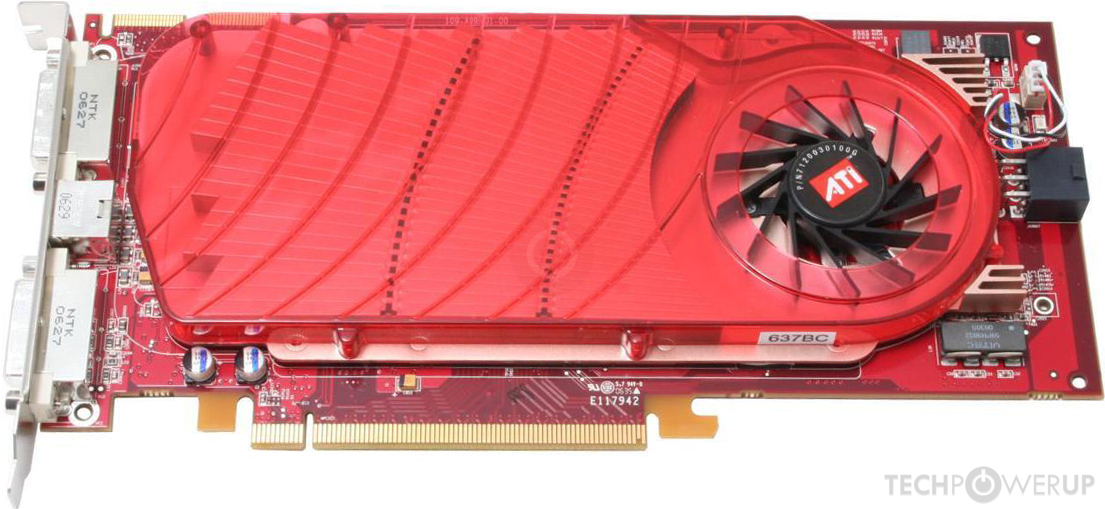
Being a single-slot card, the ATI Radeon X1950 PRO draws power from 1x 6-pin power connector, with power draw rated at 66 W maximum. Display outputs include: 2x DVI, 1x S-Video. Radeon X1950 PRO is connected to the rest of the system using a PCI-Express 1.0 x16 interface. The card measures 228 mm in length, 111 mm in width, and features a single-slot cooling solution.
Being a single-slot card, the ATI Radeon X1950 PRO draws power from 1x 6-pin power connector, with power draw rated at 66 W maximum. Display outputs include: 2x DVI, 1x S-Video. Radeon X1950 PRO is connected to the rest of the system using a PCI-Express 1.0 x16 interface. The card measures 228 mm in length, 111 mm in width, and features a single-slot cooling solution.
Graphics Processor
- GPU Name
- RV570
- GPU Variant
-
RV570 X1950
(215PADAKA12FGP)
- Architecture
- Ultra-Threaded SE
- Foundry
- TSMC
- Process Size
- 80 nm
- Transistors
- 312 million
- Density
- 1.4M / mm²
- Die Size
- 230 mm²
Graphics Card
- Release Date
- Oct 1st, 2006
- Generation
-
Radeon R500 PCIe
(X1950)
- Predecessor
- Radeon R400 PCIe
- Successor
- Radeon R600
- Production
- End-of-life
- Bus Interface
- PCIe 1.0 x16
- Reviews
- 144 in our database
Clock Speeds
- GPU Clock
- 575 MHz
- Memory Clock
-
690 MHz
1380 Mbps effective
Memory
- Memory Size
- 256 MB
- Memory Type
- GDDR3
- Memory Bus
- 256 bit
- Bandwidth
- 44.16 GB/s
Render Config
- Pixel Shaders
- 36
- Vertex Shaders
- 8
- TMUs
- 12
- ROPs
- 12
Theoretical Performance
- Pixel Rate
- 6.900 GPixel/s
- Vertex Rate
- 1.150 GVertices/s
- Texture Rate
- 6.900 GTexel/s
Board Design
- Slot Width
- Single-slot
- Length
- 228 mm
9 inches
- Width
- 111 mm
4.4 inches
- TDP
- 66 W
- Suggested PSU
- 250 W
- Outputs
- 2x DVI
1x S-Video
- Power Connectors
- 1x 6-pin
- Board Number
- 109-A99931-00
Graphics Features
- DirectX
- 9.0c (9_3)
- OpenGL
-
2.1 (full)
3.0 (partial)
- OpenCL
- N/A
- Vulkan
- N/A
- Shader Model
- 3.0
Card Notes
| Memory Variant: 512 MB |
RV570 GPU Notes
| Mobile Variant: M68 Codename: Warhol Graphics/Compute: GFX2 Display Core Engine: 1.0 Avivo Video Programmable pixel&vertex pipelines |
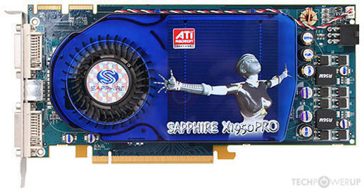
Retail boards based on this design (4)
| Name | GPU Clock | Memory Clock | Other Changes |
|---|---|---|---|
| 574 MHz | 693 MHz | 512 MB, Dual-slot | |
| 575 MHz | 690 MHz | Dual-slot | |
| 575 MHz | 690 MHz | ||
| 575 MHz | 690 MHz |


Apr 18th, 2024 02:39 EDT
change timezone
Latest GPU Drivers
New Forum Posts
- FINAL FANTASY XIV: Dawntrail Official Benchmark (47)
- What are you playing? (20451)
- EDP other basically constantly red while playing games (2)
- Realtek Modded Audio Driver for Windows 10/11 - Only for HDAUDIO (5675)
- AMD RX 7000 series GPU Owners' Club (1064)
- Will a RTX 4070 TI super bottleneck a Ryzen 9 7950X3D? (28)
- Identify my GPU - RX 570 8GB (or what?) (0)
- What's your latest tech purchase? (20253)
- 4K Gamers, How much VRAM do you have? (131)
- Your PC ATM (34483)
Popular Reviews
- Horizon Forbidden West Performance Benchmark Review - 30 GPUs Tested
- PowerColor Radeon RX 7900 GRE Hellhound Review
- ASUS GeForce RTX 4090 Matrix Platinum Review - The RTX 4090 Ti
- Fractal Design Terra Review
- Corsair 2000D Airflow Review
- Minisforum EliteMini UM780 XTX (AMD Ryzen 7 7840HS) Review
- Creative Pebble X Plus Review
- FiiO KB3 HiFi Mechanical Keyboard Review - Integrated DAC/Amp!
- ASUS GeForce RTX 4090 STRIX OC Review
- NVIDIA GeForce RTX 4090 Founders Edition Review - Impressive Performance
Controversial News Posts
- Sony PlayStation 5 Pro Specifications Confirmed, Console Arrives Before Holidays (105)
- NVIDIA Points Intel Raptor Lake CPU Users to Get Help from Intel Amid System Instability Issues (102)
- US Government Wants Nuclear Plants to Offload AI Data Center Expansion (98)
- Windows 10 Security Updates to Cost $61 After 2025, $427 by 2028 (82)
- Developers of Outpost Infinity Siege Recommend Underclocking i9-13900K and i9-14900K for Stability on Machines with RTX 4090 (82)
- TechPowerUp Hiring: Reviewers Wanted for Motherboards, Laptops, Gaming Handhelds and Prebuilt Desktops (71)
- Intel Realizes the Only Way to Save x86 is to Democratize it, Reopens x86 IP Licensing (70)
- AMD Zen 5 Execution Engine Leaked, Features True 512-bit FPU (63)