Report an Error


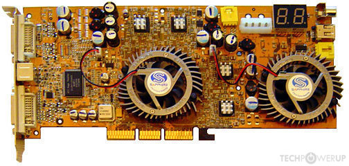
Sapphire 9800 PRO MAXX
- Graphics Processor
- R350 x2
- Pixel Shaders
- 8 x2
- Vertex Shaders
- 4 x2
- TMUs
- 8 x2
- ROPs
- 8 x2
- Memory Size
- 128 MB x2
- Memory Type
- DDR
- Bus Width
- 256 bit x2
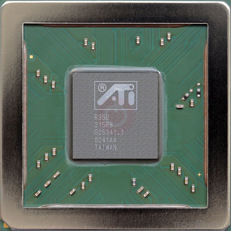
GPU
Graphics Processor
Graphics Card
- Release Date
Unknown
Sep 23rd, 2003
- Generation
-
Radeon R300
(9800)
- Predecessor
- Radeon R200
- Successor
- Radeon R400 AGP
- Production
- End-of-life
- Bus Interface
- AGP 8x
Clock Speeds
- GPU Clock
380 MHz
400 MHz (+5%)
- Memory Clock
-
340 MHz
400 MHz (+18%)
680 Mbps effective
800 Mbps effective
Memory
- Memory Size
- 128 MB
- Memory Type
- DDR
- Memory Bus
- 256 bit
- Bandwidth
-
21.76 GB/s
25.60 GB/s
Render Config
- Pixel Shaders
- 8
- Vertex Shaders
- 4
- TMUs
- 8
- ROPs
- 8
Theoretical Performance
- Pixel Rate
-
3.040 GPixel/s
3.200 GPixel/s
- Vertex Rate
-
380.0 MVertices/s
400.0 MVertices/s
- Texture Rate
-
3.040 GTexel/s
3.200 GTexel/s
Board Design
- Slot Width
- Single-slot
- TDP
- 94 W
- Suggested PSU
- 250 W
- Outputs
- 2x DVI
1x S-Video
- Power Connectors
- 1x Molex
Graphics Features
- DirectX
- 9.0 (9_0)
- OpenGL
- 2.0
- OpenCL
- N/A
- Vulkan
- N/A
- Pixel Shader
- 2.0
- Vertex Shader
- 2.0
Card Notes
| Unreleased Prototype by Sapphire |
R350 GPU Notes
| Codename: Khan Graphics/Compute: GFX2 Smart Shader 2.1 Smooth Vision 2.1 TruForm 2.0 FullStream Hyper Z III+ Video Shader Video Immersion II |
Other retail boards based on this design (1)
| Name | GPU Clock | Memory Clock | Other Changes |
|---|---|---|---|
|
Sapphire 9800 PRO MAXX

|
400 MHz | 400 MHz |
Apr 23rd, 2024 16:32 EDT
change timezone
Latest GPU Drivers
New Forum Posts
- CPB Enabled Boot Loop (3)
- Aida64 cache mem OC (4)
- No POST, and no display (7)
- Meta Horizon OS (6)
- windows 11 (4)
- Which new games will you be buying? (299)
- need help with motherboard/ ram compability certainty (5)
- My computer setup - Request for opinions (11)
- EK seems to be having major issues (26)
- DeepCool AIO LS720 RGB NOT WORKING HELP! (0)
Popular Reviews
- Horizon Forbidden West Performance Benchmark Review - 30 GPUs Tested
- Fractal Design Terra Review
- Corsair 2000D Airflow Review
- Thermalright Phantom Spirit 120 EVO Review
- Minisforum EliteMini UM780 XTX (AMD Ryzen 7 7840HS) Review
- ASUS GeForce RTX 4090 STRIX OC Review
- NVIDIA GeForce RTX 4090 Founders Edition Review - Impressive Performance
- ASUS GeForce RTX 4090 Matrix Platinum Review - The RTX 4090 Ti
- Creative Pebble X Plus Review
- MSI GeForce RTX 4090 Gaming X Trio Review
Controversial News Posts
- Sony PlayStation 5 Pro Specifications Confirmed, Console Arrives Before Holidays (116)
- NVIDIA Points Intel Raptor Lake CPU Users to Get Help from Intel Amid System Instability Issues (105)
- AMD "Strix Halo" Zen 5 Mobile Processor Pictured: Chiplet-based, Uses 256-bit LPDDR5X (101)
- US Government Wants Nuclear Plants to Offload AI Data Center Expansion (98)
- Windows 10 Security Updates to Cost $61 After 2025, $427 by 2028 (84)
- Developers of Outpost Infinity Siege Recommend Underclocking i9-13900K and i9-14900K for Stability on Machines with RTX 4090 (84)
- TechPowerUp Hiring: Reviewers Wanted for Motherboards, Laptops, Gaming Handhelds and Prebuilt Desktops (74)
- Intel Realizes the Only Way to Save x86 is to Democratize it, Reopens x86 IP Licensing (70)