Report an Error


XFX 9800 GX2 Black Edition
- PVT98UZHBU
- Graphics Processor
- G92 x2
- Cores
- 128 x2
- TMUs
- 64 x2
- ROPs
- 16 x2
- Memory Size
- 512 MB x2
- Memory Type
- GDDR3
- Bus Width
- 256 bit x2

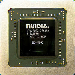
GPU
Graphics Processor
Graphics Card
- Release Date
Mar 18th, 2008
Mar 26th, 2008
- Generation
-
GeForce 9
(9800)
- Predecessor
- GeForce 8
- Successor
- GeForce 200
- Production
- End-of-life
- Bus Interface
- PCIe 2.0 x16
Clock Speeds
- GPU Clock
600 MHz
700 MHz (+17%)
- Shader Clock
1500 MHz
1700 MHz (+13%)
- Memory Clock
-
1000 MHz
1050 MHz (+5%)
2 Gbps effective
2.1 Gbps effective
Memory
- Memory Size
- 512 MB
- Memory Type
- GDDR3
- Memory Bus
- 256 bit
- Bandwidth
-
64.00 GB/s
67.20 GB/s
Render Config
- Shading Units
- 128
- TMUs
- 64
- ROPs
- 16
- SM Count
- 16
- L2 Cache
- 64 KB
Theoretical Performance
- Pixel Rate
-
9.600 GPixel/s
11.20 GPixel/s
- Texture Rate
-
38.40 GTexel/s
44.80 GTexel/s
- FP32 (float)
-
384.0 GFLOPS
435.2 GFLOPS
Board Design
- Slot Width
- Dual-slot
- TDP
- 197 W
- Suggested PSU
- 450 W
- Outputs
- 2x DVI
1x HDMI
- Power Connectors
- 1x 6-pin + 1x 8-pin
- Board Number
- P790 SKU 0,
P791
Graphics Features
- DirectX
- 11.1 (10_0)
- OpenGL
- 3.3
- OpenCL
- 1.1
- Vulkan
- N/A
- CUDA
- 1.1
- Shader Model
- 4.0
G92 GPU Notes
| PureVideo HD: VP2 VDPAU: Feature Set A |
Other retail boards based on this design (7)
| Name | GPU Clock | Memory Clock | Other Changes |
|---|---|---|---|
| 670 MHz | 1065 MHz | ||
| 650 MHz | 1025 MHz | ||
| 675 MHz | 1050 MHz | ||
| 625 MHz | 1000 MHz | ||
| 600 MHz | 1000 MHz | ||
|
XFX 9800 GX2 Black Edition

|
700 MHz | 1050 MHz | |
| 680 MHz | 1040 MHz |


Apr 24th, 2024 16:10 EDT
change timezone
Latest GPU Drivers
New Forum Posts
- Is It The 1080 TI The Best GPU Ever? (210)
- Core PL1 + GPU PL1 + Ring EDP OTHER (6)
- Meta Horizon OS (13)
- Rare GPUs / Unreleased GPUs (1875)
- What's your latest tech purchase? (20336)
- What are you playing? (20524)
- Is there a way to have 2x chrome tabs side by side in fullscreen mode? (9)
- Embracer Group is breaking into 3 smaller companies... lol who saw this coming, what a joke (11)
- Will a RTX 4070 TI super bottleneck a Ryzen 9 7950X3D? (53)
- GTX 1070 Ti - TDP Issues - Always Power Throttling (0)
Popular Reviews
- Fractal Design Terra Review
- Thermalright Phantom Spirit 120 EVO Review
- Corsair 2000D Airflow Review
- Minisforum EliteMini UM780 XTX (AMD Ryzen 7 7840HS) Review
- ASUS GeForce RTX 4090 STRIX OC Review
- NVIDIA GeForce RTX 4090 Founders Edition Review - Impressive Performance
- ASUS GeForce RTX 4090 Matrix Platinum Review - The RTX 4090 Ti
- MSI GeForce RTX 4090 Gaming X Trio Review
- MSI GeForce RTX 4090 Suprim X Review
- Gigabyte GeForce RTX 4090 Gaming OC Review
Controversial News Posts
- Sony PlayStation 5 Pro Specifications Confirmed, Console Arrives Before Holidays (116)
- NVIDIA Points Intel Raptor Lake CPU Users to Get Help from Intel Amid System Instability Issues (106)
- AMD "Strix Halo" Zen 5 Mobile Processor Pictured: Chiplet-based, Uses 256-bit LPDDR5X (101)
- US Government Wants Nuclear Plants to Offload AI Data Center Expansion (98)
- Windows 10 Security Updates to Cost $61 After 2025, $427 by 2028 (84)
- Developers of Outpost Infinity Siege Recommend Underclocking i9-13900K and i9-14900K for Stability on Machines with RTX 4090 (84)
- TechPowerUp Hiring: Reviewers Wanted for Motherboards, Laptops, Gaming Handhelds and Prebuilt Desktops (78)
- Intel Realizes the Only Way to Save x86 is to Democratize it, Reopens x86 IP Licensing (70)