Report an Error


MSI GTX 465 Golden Edition
- N465GTX-Twin-Frozr-II-Golden-Edition
- Graphics Processor
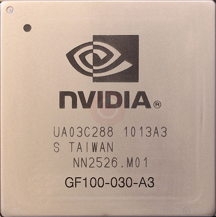
- GF100
- Cores
- 352
- TMUs
- 44
- ROPs
- 32
- Memory Size
- 1024 MB
- Memory Type
- GDDR5
- Bus Width
- 256 bit

GPU
Graphics Processor
Graphics Card
- Release Date
- May 31st, 2010
- Generation
- GeForce 400
- Predecessor
- GeForce 200
- Successor
- GeForce 500
- Production
- End-of-life
- Bus Interface
- PCIe 2.0 x16
Clock Speeds
- GPU Clock
- 608 MHz
- Shader Clock
- 1215 MHz
- Memory Clock
-
802 MHz
3.2 Gbps effective
Memory
- Memory Size
- 1024 MB
- Memory Type
- GDDR5
- Memory Bus
- 256 bit
- Bandwidth
- 102.7 GB/s
Render Config
- Shading Units
- 352
- TMUs
- 44
- ROPs
- 32
- SM Count
- 11
- L1 Cache
- 64 KB (per SM)
- L2 Cache
- 512 KB
Theoretical Performance
- Pixel Rate
- 13.38 GPixel/s
- Texture Rate
- 26.75 GTexel/s
- FP32 (float)
- 855.4 GFLOPS
- FP64 (double)
- 106.9 GFLOPS (1:8)
Board Design
- Slot Width
- Dual-slot
- Length
241 mm
243 mm
9.5 inches
9.6 inches
- TDP
- 200 W
- Suggested PSU
- 550 W
- Outputs
- 2x DVI
1x mini-HDMI 1.3a
- Power Connectors
- 2x 6-pin
- Board Number
- P1025 SKU 0008
Graphics Features
- DirectX
- 12 (11_0)
- OpenGL
- 4.6
- OpenCL
- 1.1
- Vulkan
- N/A
- CUDA
- 2.0
- Shader Model
- 5.1
GF100 GPU Notes
| PureVideo HD: VP4 VDPAU: Feature Set C GF100 has 4 GPCs each capable of 8 pixels per clock. This limits complete GPU to 32 pixels per clock and because of that it can't feed all 48 ROPs when they all require data at the same time. Additional ROPs however can be used for MSAA (because it doesn't require additional data from rasterizers, while giving more work to ROPs.) |
Other retail boards based on this design (3)
| Name | GPU Clock | Memory Clock | Other Changes |
|---|---|---|---|
| 608 MHz | 802 MHz | 2x DVI 1x HDMI 1x DisplayPort | |
|
MSI GTX 465 Golden Edition

|
608 MHz | 802 MHz | 243 mm/9.6 inches |
| 608 MHz | 802 MHz |


Apr 23rd, 2024 09:38 EDT
change timezone
Latest GPU Drivers
New Forum Posts
- EK seems to be having major issues (25)
- Odd RTX 3080 behaviour (2)
- Possible near-future 2024 Arrow Lake build.... (47)
- Windows 12 (141)
- Show us your collections thread!! (281)
- Serious bug in PHP reported! (2)
- Upgrade Build (105)
- The Official Linux/Unix Desktop Screenshots Megathread (693)
- Share your AIDA 64 cache and memory benchmark here (2913)
- My computer setup - Request for opinions (4)
Popular Reviews
- Horizon Forbidden West Performance Benchmark Review - 30 GPUs Tested
- Fractal Design Terra Review
- Corsair 2000D Airflow Review
- Thermalright Phantom Spirit 120 EVO Review
- Minisforum EliteMini UM780 XTX (AMD Ryzen 7 7840HS) Review
- ASUS GeForce RTX 4090 STRIX OC Review
- NVIDIA GeForce RTX 4090 Founders Edition Review - Impressive Performance
- ASUS GeForce RTX 4090 Matrix Platinum Review - The RTX 4090 Ti
- Creative Pebble X Plus Review
- MSI GeForce RTX 4090 Gaming X Trio Review
Controversial News Posts
- Sony PlayStation 5 Pro Specifications Confirmed, Console Arrives Before Holidays (116)
- NVIDIA Points Intel Raptor Lake CPU Users to Get Help from Intel Amid System Instability Issues (105)
- AMD "Strix Halo" Zen 5 Mobile Processor Pictured: Chiplet-based, Uses 256-bit LPDDR5X (101)
- US Government Wants Nuclear Plants to Offload AI Data Center Expansion (98)
- Windows 10 Security Updates to Cost $61 After 2025, $427 by 2028 (84)
- Developers of Outpost Infinity Siege Recommend Underclocking i9-13900K and i9-14900K for Stability on Machines with RTX 4090 (82)
- TechPowerUp Hiring: Reviewers Wanted for Motherboards, Laptops, Gaming Handhelds and Prebuilt Desktops (74)
- Intel Realizes the Only Way to Save x86 is to Democratize it, Reopens x86 IP Licensing (70)