Report an Error


SPARKLE GT 620 Low Profile
- SX620L1024HC
- Graphics Processor
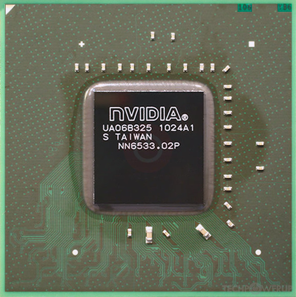
- GF108
- Cores
- 96
- TMUs
- 16
- ROPs
- 4
- Memory Size
- 1024 MB
- Memory Type
- DDR3
- Bus Width
- 64 bit

GPU
Graphics Processor
Graphics Card
- Release Date
- May 15th, 2012
- Generation
- GeForce 600
- Predecessor
- GeForce 500
- Successor
- GeForce 700
- Production
- End-of-life
- Bus Interface
- PCIe 2.0 x16
Clock Speeds
- GPU Clock
- 700 MHz
- Shader Clock
- 1400 MHz
- Memory Clock
-
900 MHz
500 MHz (-44%)
1800 Mbps effective
1000 Mbps effective
Memory
- Memory Size
- 1024 MB
- Memory Type
- DDR3
- Memory Bus
- 64 bit
- Bandwidth
-
14.40 GB/s
8.000 GB/s
Render Config
- Shading Units
- 96
- TMUs
- 16
- ROPs
- 4
- SM Count
- 2
- L1 Cache
- 64 KB (per SM)
- L2 Cache
- 128 KB
Theoretical Performance
- Pixel Rate
- 2.800 GPixel/s
- Texture Rate
- 11.20 GTexel/s
- FP32 (float)
- 268.8 GFLOPS
- FP64 (double)
- 22.40 GFLOPS (1:12)
Board Design
- Slot Width
- Single-slot
- Length
145 mm
154 mm
5.7 inches
6.1 inches
- TDP
- 49 W
- Suggested PSU
- 200 W
- Outputs
- 1x DVI
1x HDMI 1.3a
1x VGA
- Power Connectors
- None
- Board Number
- P1071
Graphics Features
- DirectX
- 12 (11_0)
- OpenGL
- 4.6
- OpenCL
- 1.1
- Vulkan
- N/A
- CUDA
- 2.1
- Shader Model
- 5.1
GF108 GPU Notes
| PureVideo HD: VP4 VDPAU: Feature Set C |
Other retail boards based on this design (11)
| Name | GPU Clock | Memory Clock | Other Changes |
|---|---|---|---|
| 700 MHz | 910 MHz | 2 GB, 188 mm/7.4 inches | |
| 700 MHz | 600 MHz | 169 mm/6.7 inches | |
| 700 MHz | 667 MHz | 169 mm/6.7 inches | |
| 700 MHz | 700 MHz | 2x DVI 1x mini-HDMI | |
| 700 MHz | 600 MHz | ||
| 700 MHz | 500 MHz | 2 GB | |
| 700 MHz | 516 MHz | 160 mm/6.3 inches | |
| 700 MHz | 516 MHz | 2 GB, 160 mm/6.3 inches | |
| 700 MHz | 667 MHz | 156 mm/6.1 inches | |
| 700 MHz | 667 MHz | 2 GB, 156 mm/6.1 inches | |
|
SPARKLE GT 620 Low Profile

|
700 MHz | 500 MHz | 154 mm/6.1 inches |


Apr 16th, 2024 07:43 EDT
change timezone
Latest GPU Drivers
New Forum Posts
- Help finding PSU Cables (7)
- Outer Worlds getting boring (12)
- Telegram for Desktop less than perfect (2)
- Visually does this GPU seem to have any problems? (8)
- FINAL FANTASY XIV: Dawntrail Official Benchmark (31)
- Samsung 870 EVO - Beware, certain batches prone to failure! (1128)
- Presonus Eris 3.5 VS Logitech Z506 (2)
- USB C to USB A hub (40)
- Which air cooler for a ryzen 9 5900x (136)
- Dromaeo: JavaScript tests (2)
Popular Reviews
- Horizon Forbidden West Performance Benchmark Review - 30 GPUs Tested
- PowerColor Radeon RX 7900 GRE Hellhound Review
- Galax GeForce RTX 4070 Super EX Review
- Fractal Design Terra Review
- ASUS GeForce RTX 4090 Matrix Platinum Review - The RTX 4090 Ti
- Corsair 2000D Airflow Review
- Minisforum EliteMini UM780 XTX (AMD Ryzen 7 7840HS) Review
- Creative Pebble X Plus Review
- FiiO KB3 HiFi Mechanical Keyboard Review - Integrated DAC/Amp!
- ASUS GeForce RTX 4090 STRIX OC Review
Controversial News Posts
- NVIDIA Points Intel Raptor Lake CPU Users to Get Help from Intel Amid System Instability Issues (102)
- US Government Wants Nuclear Plants to Offload AI Data Center Expansion (98)
- Sony PlayStation 5 Pro Specifications Confirmed, Console Arrives Before Holidays (89)
- Developers of Outpost Infinity Siege Recommend Underclocking i9-13900K and i9-14900K for Stability on Machines with RTX 4090 (82)
- Windows 10 Security Updates to Cost $61 After 2025, $427 by 2028 (79)
- TechPowerUp Hiring: Reviewers Wanted for Motherboards, Laptops, Gaming Handhelds and Prebuilt Desktops (70)
- Intel Realizes the Only Way to Save x86 is to Democratize it, Reopens x86 IP Licensing (70)
- AMD Zen 5 Execution Engine Leaked, Features True 512-bit FPU (63)