News Posts matching #55 nm

Return to Keyword Browsing

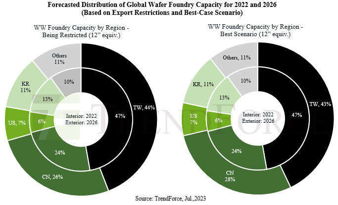
China's Share in Mature Process Capacity Predicted to Hit 29% in 2023, Climbing to 33% by 2027

TrendForce reports that from 2023 to 2027, the global ratio of mature (>28 nm) to advanced (<16 nm) processes is projected to hover around 7:3. Propelled by policies and incentives promoting local production and domestic IC development, China's mature process capacity is anticipated to grow from 29% this year to 33% by 2027. Leading the charge are giants like SMIC, HuaHong Group, and Nexchip, while Taiwan's share is estimated to consolidate from 49% down to 42%.

Expansion predominantly targets specialty processes such as Driver ICs, CIS/ISPs, and Power Discretes, with second and third-tier Taiwanese manufacturers at the forefront
Within the Driver IC sector, the spotlight is on high voltage (HV) specialty processes. As companies aggressively pursue the 40/28 nm HV process, UMC currently dominates, trailed by GlobalFoundries. Yet, SMIC's 28HV and Nexchip's 40HV are gearing up for mass production in 4Q23 and 1H24, respectively—narrowing their technological gap with other foundries. Notably, competitors with similar process capabilities and capacities, such as PSMC, and those without twelve-inch factories like Vanguard and DBHitek, are poised to face challenges head-on in the short term. This trend may also have long-term implications for UMC and GlobalFoundries.

Despite Export Ban on Equipment, China's Semiconductor Expansion in Mature Processes Remains Strong

On June 30th, the Netherlands introduced new export restrictions on advanced semiconductor manufacturing equipment. Despite facing export controls from the US, Japan, and the Netherlands, TrendForce anticipates the market share of Chinese foundries in terms of 12-inch wafer production capacity will likely increase from 24% in 2022 to an estimated 26% in 2026. Moreover, if the exports of 40/28 nm equipment eventually receive approval, there's a chance that this market share could expand even further, possibly reaching 28% by 2026. This growth potential should not be dismissed.

Several manufacturing processes including photolithography, deposition, and epitaxy will be subject to these recent export restrictions. Beginning September 1st, the export of all controlled items will require formal authorization. TrendForce reports that Chinese foundries have been primarily developing mature processes like 55 nm, 40 nm, and 28 nm. Furthermore, demand for deposition equipment can be largely met by local Chinese vendors, meaning concerns regarding expansion and development are minimal. The main limiting factor, however, remains the equipment used in photolithography.

AMD Explains the Economics Behind Chiplets for GPUs

AMD, in its technical presentation for the new Radeon RX 7900 series "Navi 31" GPU, gave us an elaborate explanation on why it had to take the chiplets route for high-end GPUs, devices that are far more complex than CPUs. The company also enlightened us on what sets chiplet-based packages apart from classic multi-chip modules (MCMs). An MCM is a package that consists of multiple independent devices sharing a fiberglass substrate.

An example of an MCM would be a mobile Intel Core processor, in which the CPU die and the PCH die share a substrate. Here, the CPU and the PCH are independent pieces of silicon that can otherwise exist on their own packages (as they do on the desktop platform), but have been paired together on a single substrate to minimize PCB footprint, which is precious on a mobile platform. A chiplet-based device is one where a substrate is made up of multiple dies that cannot otherwise independently exist on their own packages without an impact on inter-die bandwidth or latency. They are essentially what should have been components on a monolithic die, but disintegrated into separate dies built on different semiconductor foundry nodes, with a purely cost-driven motive.

Semiconductor Fab Order Cancellations Expected to Result in Reduced Capacity Utilization Rate in 2H22

According to TrendForce investigations, foundries have seen a wave of order cancellations with the first of these revisions originating from large-size Driver IC and TDDI, which rely on mainstream 0.1X μm and 55 nm processes, respectively. Although products such as MCU and PMIC were previously in short supply, foundries' capacity utilization rate remained roughly at full capacity through their adjustment of product mix. However, a recent wave cancellations have emerged for PMIC, CIS, and certain MCU and SoC orders. Although still dominated by consumer applications, foundries are beginning to feel the strain of the copious order cancellations from customers and capacity utilization rate has officially declined.

Looking at trends in 2H22, TrendForce indicates, in addition to no relief from the sustained downgrade of driver IC demand, inventory adjustment has begun for smartphones, PCs, and TV-related peripheral components such as SoCs, CIS, and PMICs, and companies are beginning to curtail their wafer input plans with foundries. This phenomenon of order cancellations is occurring simultaneously in 8-inch and 12-inch fabs at nodes including 0.1X μm, 90/55 nm, and 40/28 nm. Not even the advanced 7/6 nm processes are immune.

Polyn Technology Delivers NASP Test Chip for Tiny AI

Polyn Technology announced today that its first Neuromorphic Analog Signal Processor (NASP) chip is packaged and evaluated, demonstrating proof of the technology's brain-mimicking architecture. It is the first Tiny AI true analog design to be used next to sensors. Polyn Technology is an innovative provider of ultra-low-power-performance NASP technology and a producer of unique Tiny AI chips and their associated IP. "This achievement validates the intensive work of our multinational team," said Aleksandr Timofeev, CEO and founder of Polyn Technology. "Our chip represents the most advanced technology bridging analog computations and the digital core. It is designed with neuroscience in mind, replicating pre-processing the primary cortical area of the human brain does at the periphery before learning at the center."

The NASP chip enables full data processing disaggregation between the sensor node and the cloud; it truly embodies the Tiny AI concept. The NASP test chip contains several neural networks. The chip is implemented in 55 nm CMOS technology. Its design proves the NASP "neuron" model as well as the scalability of the technology and efficiency of the chip design automation tools developed by Polyn. "Our first chip is created from trained neural networks by NASP Compiler and synthesis tools that generated Netlist and the silicon engineering files from the software math model simulation. We will continue to refine our technology for creation of new generation chips," said Yaakov Milstain, COO of Polyn. Polyn anticipates the chip will be available to customers in the first quarter of 2023 as its first wearables product, with a fusion of PPG and IMU sensors for the most accurate heart rate measurement along with recognition and tracking of human activity.

Foundry Revenue Projected to Reach Historical High of US$94.6 Billion in 2021 Thanks to High 5G/HPC/End-Device Demand, Says TrendForce

As the global economy enters the post-pandemic era, technologies including 5G, WiFi6/6E, and HPC (high-performance computing) have been advancing rapidly, in turn bringing about a fundamental, structural change in the semiconductor industry as well, according to TrendForce's latest investigations. While the demand for certain devices such as notebook computers and TVs underwent a sharp uptick due to the onset of the stay-at-home economy, this demand will return to pre-pandemic levels once the pandemic has been brought under control as a result of the global vaccination drive. Nevertheless, the worldwide shift to next-gen telecommunication standards has brought about a replacement demand for telecom and networking devices, and this demand will continue to propel the semiconductor industry, resulting in high capacity utilization rates across the major foundries. As certain foundries continue to expand their production capacities this year, TrendForce expects total foundry revenue to reach a historical high of US$94.6 billion this year, an 11% growth YoY.

NVIDIA GeForce GTX 880 and GTX 870 to Launch This Q4

NVIDIA is planning to launch its next high performance single-GPU graphics cards, the GeForce GTX 880 and GTX 870, no later than Q4-2014, in the neighborhood of October and November, according to a SweClockers report. The two will be based on the brand new "GM204" silicon, which most reports suggest, is based on the existing 28 nm silicon fab process. Delays by NVIDIA's principal foundry partner TSMC to implement its next-generation 20 nm process has reportedly forced the company to design a new breed of "Maxwell" based GPUs on the existing 28 nm process. The architecture's good showing with efficiency on the GeForce GTX 750 series probably gave NVIDIA hope. When 20 nm is finally smooth, it wouldn't surprise us if NVIDIA optically shrinks these chips to the new process, like it did to the G92 (from 65 nm to 55 nm). The GM204 chip is rumored to feature 3,200 CUDA cores, 200 TMUs, 32 ROPs, and a 256-bit wide GDDR5 memory interface. It succeeds the company's current workhorse chip, the GK104.

ARM and GLOBALFOUNDRIES Collaborate to Enable Devices on 20 nm and FinFET

GLOBALFOUNDRIES and ARM today announced a multi-year agreement to jointly deliver optimized system-on-chip (SoC) solutions for ARM processor designs on GLOBALFOUNDRIES' 20-nanometer (nm) and FinFET process technologies. The new agreement also extends the long-standing collaboration to include graphics processors, which are becoming an increasingly critical component in mobile devices. As part of the agreement, ARM will develop a full platform of ARM Artisan Physical IP, including standard cell libraries, memory compilers and POP IP solutions. The results will help enable a new level of system performance and power-efficiency for a range of mobile applications, from smartphones to tablets to ultra-thin notebooks.

The companies have been collaborating for several years to jointly optimize ARM Cortex-A series processors, including multiple demonstrations of performance and power-efficiency benefits on 28nm as well as a 20nm test-chip implementation currently running through GLOBALFOUNDRIES fab in Malta, N.Y. This agreement extends the prior efforts by driving production IP platforms that will enable customer designs on 20nm and promote rapid migration to three-dimensional FinFET transistor technology. This joint development will enable a faster time to delivering SoC solutions for customers using next-generation ARM CPUs and GPUs in mobile devices.

Galaxy Readying Another GeForce 9600 GT Low Power Accelerator

Galaxy is readying another variant of the GeForce 9600 GT Low Power Edition. Prior to this, the company had launched the 9600 GT Low Power, Low Profile (LPLP edition), and the 9600 GT Green Edition. Unlike the two, the new variant uses a full-height PCB, and a cooler made by Cooler Master, that doesn't span into more than one expansion slot.

The card draws all its power from the PCI-Express slot, and uses a 2+1 phase power design. Under the cooler is a 55 nm G94 GPU, with clock speeds of 600/1625 MHz (core/shader). The 512 MB of 256-bit GDDR3 memory is passively cooled under the cooler's air-flow. It is clocked at 900 MHz (1800 MHz DDR). Output is care of DVI, D-Sub, and audio-relayed HDMI connectors. It's pricing and availability isn't disclosed yet.

NVIDIA Outsources 40 nm to Foundry Partners in Q2

With rival AMD having a production-grade 40 nm graphics processor, and UMC's recent announcement of being ready with a high-performance 40 nm manufacturing node, the conditions are increasingly favourable for NVIDIA to flag-off large-scale production of 40 nm GPUs. According to Chinese print-media Commercial Times, the company set its foundry outsourcing schedule for within Q2 2009, with TSMC and UMC being the regular foundry-partners.

Within this quarter, NVIDIA will start mass-production of the entry-level GT218, high-end mobile GT215 and mainstream desktop GT214 and GT216 GPUs. Additionally, the company may also expand its output for the 55 nm G200b high-end GPU.

EVGA Adds SuperClocked Variant to GeForce GTX 275 Lineup

Having begun its GeForce GTX 275 lineup with two cards: the 896 MB base-model (896-P3-1170-AR) and its 1792 MB twin (017-P3-1175-AR), EVGA sought to expand it with factory-overclocked models with its usual overclock-grading scheme. The first in its series is the SuperClocked (SC) model (896-P3-1171-AR). The card features the design and color-theme EVGA used for its GeForce GTX 260 55 nm series. It features 240 stream processors, 896 MB of GDDR3 memory across a 448-bit wide interface, and support for 3-way SLI.

Featuring a tier-one factory overclock, the card comes with clock speeds of 648 MHz (core), 1458 MHz (shader) and 2376 MHz (memory), against the reference clock speeds of 633/1404/2268 MHz (core/shader/memory). Put on pre-order by the EVGA store, the card is set to retail for US $269.99.

GeForce GTX 200M, GTS 100M Series Unveiled

Reigning supreme again in the desktop segment, NVIDIA is looking forward to taking the wraps off its GeForce GTX 200M mGPU series. The new GPU series looks to up the performance offer by 50%, as claimed by the company. In the league are GeForce GTX 280M, GTX 260M and GTS 160M. Before you infer from the product names that at least two of them are based on the G200 graphics processor, let us break it to you, they're not. The entire series is based on the 55 nm G92b series. The 55 nm manufacturing technology seems to have facilitated some jumps in reference clock speeds.

Gigabyte Readies Passive-Cooled GeForce 9600 GT Green Edition Accelerator

NVIDIA sought to give the GeForce 9600 GT a refresh with a new SKU, the 9600 GT Green Edition, that makes use of the reduced thermal footprints of the 55 nm G94 graphics core, and slightly reduced clock speeds, to result in energy-efficient graphics cards. Some of these do not require the 6-pin PCI-E power input. Gigabyte has its first accelerator based on this core, the GV-N96TSL-1GI. The company goes a step ahead in exploiting the thermal characteristics of the core, to come up with a silent-cooler design.

The cooler which Gigabyte refers to as "Silent Cell", consists of a central GPU contact block from which heatpipes emerge, conveying heat to an aluminum fin array that spans across the full length of the card. A part of it even protrudes out of the back-plate. The cooler relies on convectional currents of the air inside the case to draw heat from the fins, and leave the case through the backplate. Cooling aside, Gigabyte got generous with the amount of memory: 1 GB of GDDR3 across a 256-bit wide bus. Perhaps it compensates for the slightly reduced clock speeds, the extant to which, isn't known as of now. The card will hit shelves shortly, by when we could tell its price.

Mobility Radeon HD 4570 Sneaks In

Close to ten days before ATI's Mobility Radeon HD 4000 series rolls out at the upcoming CeBIT event, one of its eggs seems to have hatched a little early. Dell's Indian website has already started listing it in the specifications of the Studio 15 notebook. Enter Mobility Radeon HD 4570. This mGPU is derived from the 55 nm RV710 graphics processor, and intends to be a handy performance boost over integrated graphics. It features 80 stream processors, 8 texture memory units, and 4 raster operations units. It connects to GDDR3, DDR2 memory using its 64-bit wide memory bus. The card used in Dell's Studio 15 sports 256 MB of memory. The mGPU is expected to outperform competing NVIDIA G110M by 20~30%, while keeping its TDP rating at a mere 13 W. Once formally announced, one could expect to hear more about this mGPU.

Inno3D Announces GeForce GTX 260 with FreezerX2

Inno3D are excited to launch the Inno3D GeForce GTX 260 with FreezerX2 cooler that offers double the cooling performance and better value for your buck.

FreezerX2 Features
  • Dual 8 cm ball bearing PWM fan, cooling power x 2
  • DHT Technology, cooling efficiency x 2
  • 2 mm fin distance, airflow x 2
  • Smooth sanded base, contact area x 2
  • Triple heatpipe cooling performance
  • 55 nm Manufacturing Process
  • Less power consumption with 175 W

RV790 Built on Improved 55 nm Manufacturing Process

It is clear now, that AMD's next performance GPU, the RV790 will be built on the 55 nm manufacturing process. To build on this information, sources tell German website Hardware-Infos that one of the factors that will help the new GPU perform better and run at higher clock-speeds than its predecessor, the RV770 does, is the newer improved 55 nm manufacturing process it will be built on. Going by the foundry-partner codename "55GT", the RV790 may get a little help from its superior silicon fabrication, which invariably makes it more expensive to manufacture.

One of the reasons behind why AMD is starting its 40 nm GPU lineup with a mainstream GPU such as RV740, is that the 40 nm process needs further development by foundry companies. It hasn't developed to the level that safely permits manufacturing high-end GPUs with stellar transistor-counts. For the same reason, NVIDIA's 40 nm conquest will be flagged off by the entry-level GT218 GPU. High-density circuits built on the current 40 nm process are known to be very prone to electrical leakage.
Return to Keyword Browsing
Apr 18th, 2024 12:18 EDT change timezone

New Forum Posts

Popular Reviews

Controversial News Posts