News Posts matching #G92
Return to Keyword Browsing

Logitech, a leading innovator of gaming peripherals, today announced the Logitech G920 Driving Force, its first force feedback racing wheel available for Xbox One, as well as PC, will be available this fall. Built for precision racing and long-lasting reliability, the Logitech G920 Driving Force features Logitech's powerful dual-motor force feedback transmission with anti-backlash helical gearing, hand-stitched leather-wrapped rim, and stainless steel throttle, brake, and clutch pedals. The wheel is also compatible with the optional Driving Force Shifter, a six-speed manual gear stick with push-down reverse. This is the first Logitech racing wheel available for Xbox One.
"The G920 is the wheel fans have been asking for on Xbox One," said Ujesh Desai, general manager of the Logitech gaming business. "We built on our history and legacy of previous generation driving wheels to deliver on a truly immersive experience for Xbox One gamers. I personally can't wait to get behind our new wheel to play Forza Motorsport 6."

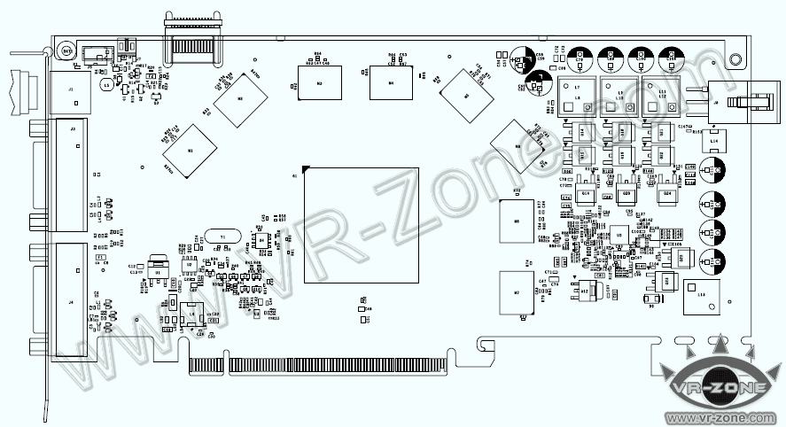
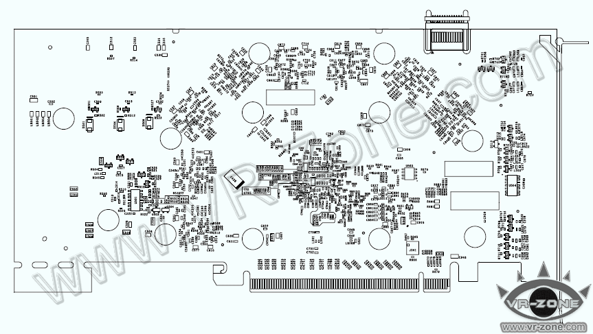
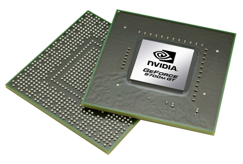
In the weeks to come, NVIDIA will release yet another graphics card based on the G92 graphics processor: the GeForce GTS 240, which bears resemblance with the 8800 GT and 9800 GT. The G92 GPU has near-identical specifications to the said graphics cards, except for that the 55 nm G92b GPU will be used, and with higher reference clock speeds of 675/1674/975 MHz (core/shader/memory). To seat the new GPU, NVIDIA has designed a new reference PCB, the P361 internally called D10P2. The schematic drawings of this has been sourced by VR-Zone.
The P361 PCB covers the basics of accommodating the G92b and eight GDDR3 memory chips connected to the GPU across a 256-bit wide bus. The distinct features of the PCB lie with its VRM area, with a 3+1 phase design. The PCB draws power from a 6-pin PCI-Express power connector. Over to the connectors department, the usual two arrangement of two DVI and one composite is present. There is a single SLI bridge connector for 2-way SLI. With the 55 nm GPU being arguably as cool or cooler than the 65 nm G92 with lower reference clock speeds, one can expect a single slot cooler design to be employed.
Desktop replacement laptop specialists Eurocom is said to be preparing the first mobile platform featuring a NVIDIA GT2xx-series (tenth generation NVIDIA GPU) multi-GPU graphics subsystem. The company's next-generation M980U Emperor already
listed on the company website, is specified to hold two Gxx-class GPUs. The company can claim this to be the first mobile platform to even feature a Gxx GPU, let alone a multi-GPU setup.
In its report, GPU Café notes that with GT2xx based mobile GPUs planned for the later half of this year, one can expect the GPUs on the Eurocom notebook to be based on the GT215 GPU, a performance-class GPU that is expected to replace the G92 series GPUs. The GT215 will be built on the 40 nm manufacturing process, from which one can expect energy efficiency. The rest of the notebook's specifications include a Core 2 Extreme processor, and uses the NVIDIA MCP79xi SLI core-logic, 1920×1080 px HD display, up to 8 GB of DDR3 memory and 1.5 TB of storage. Incidentally, Eurocom is also one of the first desktop replacement vendors to be preparing an Intel Core i7-based notebook.
Where invention pauses, innovation takes over. This seems to be the case with NVIDIA's initiative to release "Green Edition" products of some of its popular GPUs, which brandishes energy-efficiency. NVIDIA's move to release revisions of the G92 and G94 GPUs built on the newer 55 nm process, coupled with clock-speed and core voltage reductions, seems to have made it possible for manufacturers to redesign the cards in a way that they end up being not only energy efficient, but also cheaper to produce.
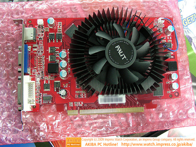
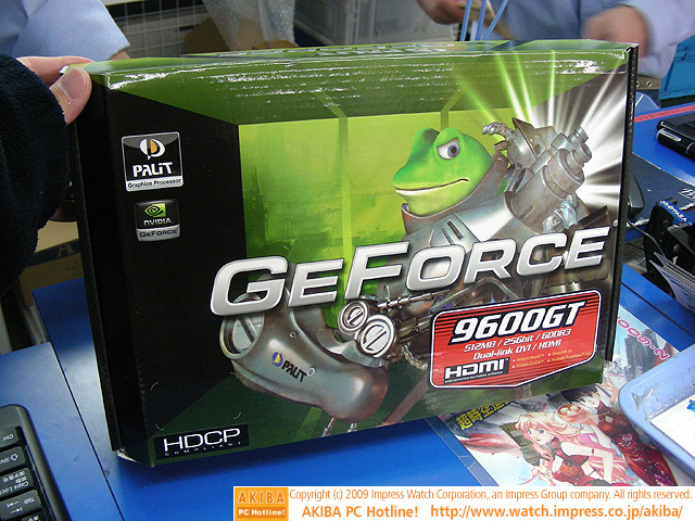
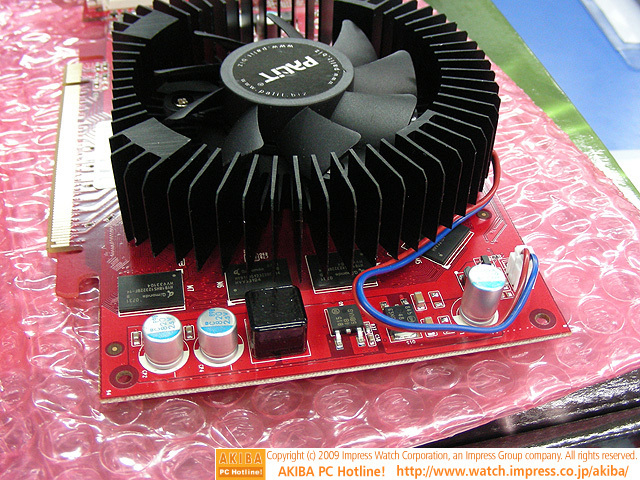
Palit seems to be one of the first to be out with a 9600 GT Green Edition accelerator that lacks a 6-pin PCI-Express power input. The card has reached retail channels in Japan, pictured by AKIBA. The card uses a core clock speed of 600 MHz, with its 512 MB of GDDR3 memory clocked at 900 (1800 DDR) MHz. The card uses Palit's regular radial GPU cooler design. It draws all its power from the PCI-Express slot. It lacks an SLI connector. Output options include DVI, D-Sub and HDMI. It is priced at ¥ 7980 (around US $86.7).
NVIDIA is going ahead with the launch schedule of the GeForce GTS 200 series, that consist of products based on the current-generation G92 GPU. It is known that the GTS 240 and GTS 250 are re-branded 9800 GT and 9800 GTX+ respectively. The 9800 GTX+ SKU will officially be renamed GTS 250 on March 3. One can expect NVIDIA partners to come up with cheaper SKUs that fit into the US $ 130 range, lower than the current $150 range 9800 GTX+ and ATI Radeon HD 4850 compete in.
The GTS 240 on the other hand, will be introduced soon with a newer price-range of around $100, lower than the $120 mark the 9800 GT revolves around. This should make it more competitive against the Radeon HD 4830, which is currently winning in the price/performance figure. Additionally, the company is preparing a GeForce 9800 GT Green Edition, which carries forward the design methodology of the 9600 GT Green Edition: lowering the GPU voltage and slightly reducing the clock speeds. It is expected to carry clock speeds of 550/1375/900 MHz (core/shader/memory) against the reference 9800 GT specifications of 600/1500/900 MHz. The new SKU might be priced at a premium over the GTS 240, at around $ 120.
In the weeks to come, next month to be more precise, NVIDIA will officially rename its G92-based graphics cards series. Amongst the "new" SKUs that have surfaced so far, NVIDIA adds the GeForce GTS 250, or present-day GeForce 9800 GTX+. In a bid to garner support from its partners, NVIDIA issued a circular that includes the following statement:
GeForce GTS 250 carries over the same specs and features of 9800 GTX+, and hence the same GPU, memory, board, PCB, and thermal solution. AIC's should be confident in purchasing GPU's, PCB's, and other materials, since the only change is a new VBIOS to implement the new branding.
The GTS 250 model will be accompanied by yet another rebranding: GeForce GTS 240, present-day GeForce 9800 GT and GeForce 8800 GT. The GeForce 9800 GTX+ was released in July 2008, to compete with ATI's Radeon HD 4850. It was an evolution of the GeForce 9800 accelerator, to which it was built on a newer manufacturing process that facilitated higher clock speeds. NVIDIA is likely to choose CeBIT as the ideal launch-pad for its new series of graphics cards.
As NVIDIA celebrates the launch of its two new flagship products: the GeForce GTX 295 and GeForce GTX 285, Sparkle made an addition to its mainstream graphics lineup with a 1 GB variant its GeForce 9600 GSO accelerator (model: SX96SO1024D3-HM). Traditionally, the G92 graphics processor in the 8800 GS, 9600 GSO should have a 192-bit memory bus, but with this particular card, Sparkle chose a 128-bit memory bus and added 1 GB of GDDR3 memory.
The card features a dual-slot cooler for the GPU. Its core is clocked at 550 MHz. Its 96 stream processors are clocked at 1375 MHz. The memory runs at 800 MHz (1600 MHz DDR). It supports NVIDIA CUDA and PhysX technologies and is SLI capable. It will be priced around US $100.
NVIDIA is seems to be recycling a broader range of existing GPUs with new branding that merely some mainstream GPUs such as the G92. According to a set of advertisements by a channel vendor, of Acer and Packard Bell PCs, they feature the GeForce G 100, GeForce GT 120 and GeForce GT 130. These graphics cards feature 512 MB, 1 GB and 1.5 GB of memory respectively and fill the entry-level graphics cards lineup.
From the information TechConnect Magazine gathered about these, they are rebranded variants of GeForce 9400, GeForce 9500 GT and GeForce 9600 GSO (aka GeForce 8800 GS). This new naming scheme will be operationalised by the end of this month, towards February, around the same time when another portion of graphics cards based on the G92 GPU get rebranded to the GeForce GTS series.
The NVIDIA G92 graphics processor has had the reputation of spanning across two generations of GeForce graphics accelerators, which could well become three with talk about NVIDIA executing another re-branding to products based on the GPU. The re-branding will use the B1 revision of the G92 GPU (aka G92b), which is known to have been manufactured on the 55nm fabrication process, along with the 65nm A1 revision.
The new series created will include two SKUs based on the G92, the GeForce GTS 240 and GeForce GTS 250. These are the 112 SP and 128 SP variants of the G92 core, presently branded under 8800/9800 GT and 8800 GTS 512, 9800 GTX/GTX+ respectively. NVIDIA looks to capitalise on the sales improvement the GTX 200 series has seen for the past two or so months now, by giving it a present-generation branding. The re-branding, or rather, releasing products with the new naming scheme is said to be operationalised by February 2009.
After releasing yet another unofficial driver today, NVIDIA kind of revealed the new naming scheme for its video cards. Three lines from the latest NVIDIA driver release 178.15 suggest the new naming scheme:
NVIDIA_G92.DEV_0615.1 = "NVIDIA GeForce GTS 150"
NVIDIA_G94.DEV_0626.1 = "NVIDIA GeForce GT 130"
NVIDIA_G96.DEV_0646.1 = "NVIDIA GeForce GT 120"
All GeForce 9800 series powered by the G92 GPU will be renamed to GeForce GTS 15x, while the GeForce 9600 and 9500 (G94 and G96) cards will be known as GeForce GT 130 and GT 120. The new naming system is expected to become formal in two weeks time.
A product change notification (PCN) document by NVIDIA The Inquirer
claims to have access to, indicates changes to the bump materials of several NVIDIA graphics processors (GPUs). Affected by this change are popular GPUs such as G92 and G92b (55nm). Changes include replacement of a High-Pb solder (95% Pb / 5% Sn) bump material with Eutectic Solder (63% Sn / 37% Pb). Bumps are those parts of the die that establish electrical contact with the leads/pins of the FC-BGA package. Failures of these bumps are irreparable leading to permanent damage. This follows several events that lead to NVIDIA owning up defects in certain mobile graphics and MCP parts.
Implications of this PCN are:
- Current G92 and G92b are weaker and could be subject to failures similar to those products already diagnosed with failing packages and official announcements issued.
NVIDIA has recently been experiencing higher-than-normal failure rates with some of its GPUs. Charlie Demerjian from The Inq. speculates that NVIDIA could actually have a much larger problem than what it admits to - it is quite possible, according to Demerjian, that not only mobile GPUs are affected, but the desktop G92 and G94 could also carry the fault.
The failures, some sources say, are caused by a solder bump that connects the I/O termination of the silicon chip to the pad on the substrate. In Nvidia's GPUs, this solder bump is created using high-lead. A thermal mismatch between the chip and the substrate has substantially grown in recent chip generations, apparently leading to fatigue cracking. What supports the theory that a high-lead solder bump in fact is at fault is the fact that Nvidia ordered an immediate switch to use eutectic solders instead of high-lead versions in the last week of July. Eutectic solders are believed to solve the problem of fatigue cracking.
NVIDIA has released two lines of high performance graphics processors (GPU) for the notebook PC market, the GeForce 9800M series and the 9700M series. These are sub-classified into GT and GTS for the 9700M and GT, GTS and GTX for the 9800M. These new GPUs provide a wide range of options for manufacturers to choose from and design high-performance gaming and multimedia notebooks.
These 9800M GTX GPU is based on the same G92 core, and will outperform its previous generation 8800M GTX that also happens to be based on the same core. The rest are based on the G94 and the newer G96 cores. These GPUs are CUDA compliant and will be able to accelerate game physics using the PhysX API. They support NVIDIA Hybrid Power technology. Simply put, on notebooks with integrated graphics processors (IGP) along with these GPUs, the system will be able to switch over to the IGP when not gaming, and switch over to the GPU when heavy graphics tasks are running (such as gaming, 3D rendering, HD Video acceleration, etc.). Speaking of video, these GPUs support Powervideo HD technology, includes VP2 acceleration. There's no information on these GPUs' fabrication technology yet. Specifications provided below.
With the cost of manufacture for a standard G200 die reaching up to US $110, thanks to yields as low as 40 per cent, NVIDIA seems to be in a rush for a 55nm revamp of its current GPUs. While nothing revolutionary is on the cards, and with 55nm G92b already in the making, NVIDIA plans to revamp its G200 graphics processors to the 55nm fab process, increasing yields up to 50 per cent. At 55nm, the G200 die will be effectively reduced to 470 sq. mm, implies 120 dice on a 300mm wafer.
The pace at which things are moving is having the partners red-eyed. NVIDIA's new Unilateral Minimum Advertised Price Policy (UMAP) has limited partners' playing field and minimizes competition between them. When NVIDIA at the same time decides to launch new cards based on existing cores, at lower prices, partners get upset over diminishing earnings. Add to that AMD's new RV770 chip is looking very tempting to some of these partners.
In order to take care of the 65nm GeForce 8800 GT and GTS 512 shortages, NVIDIA is currently negotiating with Taiwan Semiconductor Manufacturing Company (TSMC) to increase their wafer orders next year, according to DigiTimes. NVIDIA is planning to increace its supply by around 15% higher than the volume in the fourth quarter of this year.
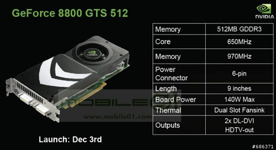
It would seem as though NVIDIA is celebrating the day that I get my full drivers license, sans passenger restrictions, by releasing the revamped NVIDIA GeForce 8800GTS 512, based on the impressive G92 micro-architecture. The new 8800GTS 512 will only come in one flavor, which, as the name suggests, will sport 512MB of 256-bit VRAM. This is opposed to the previous versions, which ship with either 320MB or 640MB of 320-bit VRAM. The new 8800GTS 512 will come with 128 Stream processors, a welcome improvement from the previous 96 Stream processors. The new 8800GTS also has another welcome surprise: an engine clock of 650MHz, higher than any 8800 series GPU before it. Current rumor has it that the 8800GTS 512's 512MB of VRAM will be clocked at roughly 1.96GHz. The 8800GTS 512 should be available on December 11th for between $299 and $349 USD.
After the success of the 8800 GT, rumours of a new 8800 GTS based on the G92 core have been on the net for a few weeks now. Now some pictures have been leaked onto the internet, along with some extra specs. It was already known to feature 128 enabled stream processors, and the latest specs claim that the new card will also have a 650MHz core clock speed, shaders at 1625MHz, 512MB memory at 1940MHz and will be nine inches long. Its official release date is said to be December 3rd, with a price tag somewhere between $299 and $349.
NVIDIA has accidently listed something on one of its web pages which would seem to support the story posted
two days ago regarding the possibility of a new 8800 GTS based on the same G92 graphics processor as the 8800 GT. Originally shown on
this page (although it's now been removed), NVIDIA let slip that it may be planning a 512MB 8800 GTS, which would seem to agree with the idea of a 256-bit version of the card. Admittedly it's not concrete evidence, but it definitely sounds suspiciously like a G92 8800 GTS could well be on the cards. The extract in question is shown at the bottom of the screenshot, and reads as follows:
5. HD DVD / Blu-ray Video Playback on NVIDIA GeForce 8800 GTS 512MB and 8800 GT is classified as Excellent. HD DVD / Blu-ray Video Playback on NVIDIA GeForce 8800 Ultra, GeForce 8800 GTX and GeForce 8800 GTS 320MB/640MB are classified as Good.
So it might be worth waiting before buying an 8800 GT if these cards are just around the corner.
After the success of the new GeForce 8800 GT, it looks like NVIDIA could have another card based on the same G92 core planned for later this year. Dubbed the new 8800 GTS (yes, I know it's confusing - hopefully that will change) the new G92 card will feature 128 shader units instead of the 112 on the 8800 GT, which would suggest they could well exist on current 8800 GT cards and have been disabled for marketing or yield purposes. As it features a 256-bit memory interface it will go back to the more common 512MB and 1024MB memory blocks, and given how impressively the 8800 GT performs it's expected it may be able to surpass NVIDIA's 8800 GTX and possibly even the Ultra - NVIDIA's two best cards. The card is expected to launch just after AMD's Radeon HD 3800, and could well spoil the show for AMD if it performs as well as the speculation suggests.
NVIDIA Announces 112 SP 8800 GTS Works w/ Original 8800 GTS In SLI
NVIDIA told their AICs not to market the new Geforce 8800 GTS 640MB as a card that has 112 SPs on board (upgraded from previous 96 SPs) but Partners can label it as a special edition, or OC edition. Also the new 112 SP 8800 GTS will still work with the original 96 SP variants in SLI configurations. Further NVIDIA stressed that they will not offer an upgraded 112 SP 8800 GTS in 320MB configurations.

According to some "highly ranked sources", the RV670 is beating NVIDIA's G92 in preliminary benchmarks. When the two reference boards are pitted against each other in an epic battle of 3Dmark06, the RV670 earns 11,400 3DMarks, and the G92 earns 10,800 3DMarks. If these benchmarks are even remotely accurate, this would prove that the new mid-range parts from both companies will be worthy competitors to the high-end parts. As comparison, the current 8800Ultra, which retails for about $600USD now, gets 12,500 in 3DMark06. Hopefully, with driver optimizations and finalized retail board designs, we will see a feisty fight for the 3DMark06 crown, and marked performance increases.
VR-Zone has learned that the G92 reference card is to be the same length as the GeForce 8800GTS measuring in at nine inches long. The PCB version is P393 and will have 1ns DDR3 memory arranged in a 16MBx32x8PCS array. The card will output HDTV, HDCP, DVI, but no display port has been mentioned yet.
VR-Zone has learned more about the upcoming NVIDIA G92 where the official marketing name is most likely to be GeForce 8700 GTS. As revealed earlier, G92 is 65nm based and has 256-bit memory bus width. The reference 8700 GTS card has 8-layer PCB and comes with 512MB GDDR3 1ns memory clocked between 900Mhz and 1GHz. Core clock is unknown yet.
NVIDIA's G92 mid-range graphics chip is provisionally set to launch on November 12th this year, while the launch date of the entry-level G98 still remains unknown, according to
DigiTimes. NVIDIA plans to replace the GeForce 8800GTS series with the G92, while the G98 will replace entry-level products in the GeForce 8 series. The G92 will support PCI Express 2.0, HDMI, PureVideo Gen 3 and Display Port, while the chip will adopt a 65nm process. Taiwan Semiconductor Manufacturing Company (TSMC) will manufacture the chips. Despite the new chip designs, G92 and G98 can only be considered an update of the GeForce 8 series since they will not include any major changes.
Christmas is coming up fast once more and rumor has it, that NVIDIA plans to release their new graphic cards in November, just in time for the holiday rush. The NVIDIA G92, possibly called GeForce 9800 GTX will have 1 billion transistors and could cost somewhere around 549 - 649 USD, while the GTS should only set you back 399 to 449 USD. Take a look at the spec's after the break.