Sapphire Intros GDDR4 Memory-Equipped Radeon HD 4670
The Radeon HD 4670 graphics processor made itself some place in the sub-$100 graphics market. AMD's partners maintained profitability as the production costs of this accelerator remained low. Its opponent, the GeForce 9600 GSO, though available in its price-range makes it difficult for its manufacturers to sell at low price-points owing to it being based on the G92 graphics processor. Eventually, NVIDIA found a way around with releasing the GeForce 9600 GSO+ SKU, where the G94 GPU with reduced shader core count was employed. This made sure NVIDIA's partners brought in aggressive pricing to counter the Radeon HD 4670.
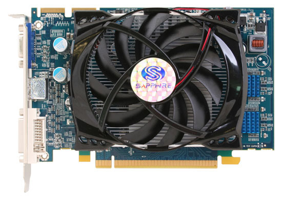
Sapphire on its part, put innovation to the table and attempted to spice-up the specifications sheets using the "GDDR4" moniker. The company released the first Radeon HD 4670 accelerator that uses 512 MB of GDDR4 memory across a 128-bit memory bus. The new graphics card features a shorter than usual PCB. It uses a central aluminum-based GPU cooler, with memory chips being cooled by heatsinks. The GPU is clocked at 750 MHz, with the memory clocked at 2200 MHz, a 200 MHz increment over the reference specs. It provides outputs in the form of a D-Sub, a DVI and a HDMI connector. It is priced as low as 75€.

Sapphire on its part, put innovation to the table and attempted to spice-up the specifications sheets using the "GDDR4" moniker. The company released the first Radeon HD 4670 accelerator that uses 512 MB of GDDR4 memory across a 128-bit memory bus. The new graphics card features a shorter than usual PCB. It uses a central aluminum-based GPU cooler, with memory chips being cooled by heatsinks. The GPU is clocked at 750 MHz, with the memory clocked at 2200 MHz, a 200 MHz increment over the reference specs. It provides outputs in the form of a D-Sub, a DVI and a HDMI connector. It is priced as low as 75€.