News Posts matching #Graphics CoreNext

Return to Keyword Browsing

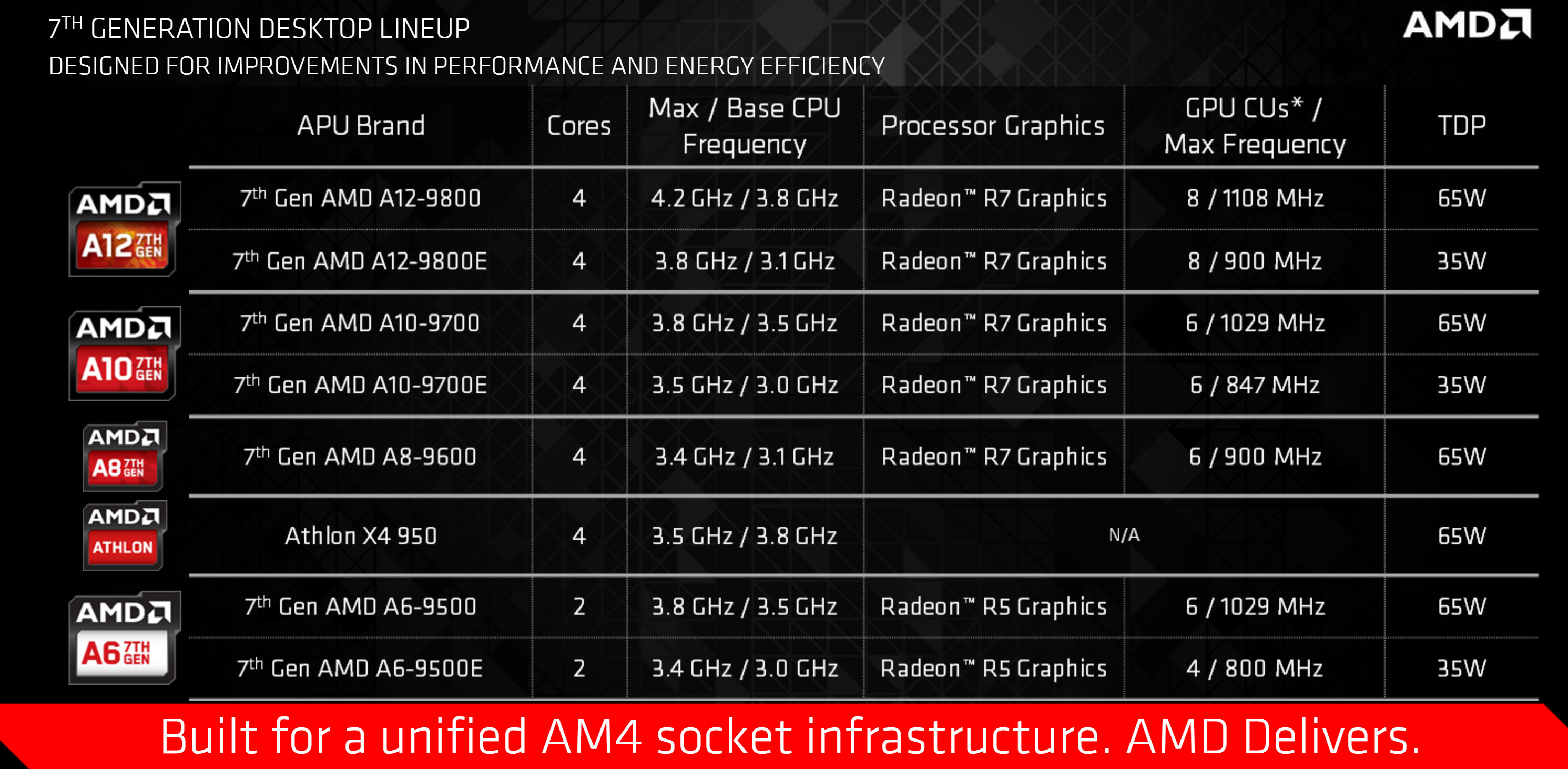
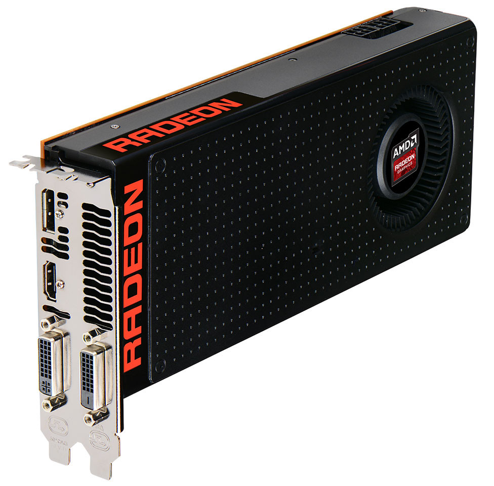
NimeZ Unofficial Radeon Drivers 22.7.1 Bring Noise Suppression Tech to Pre-RDNA GPUs

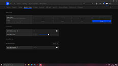
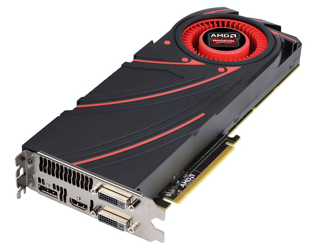
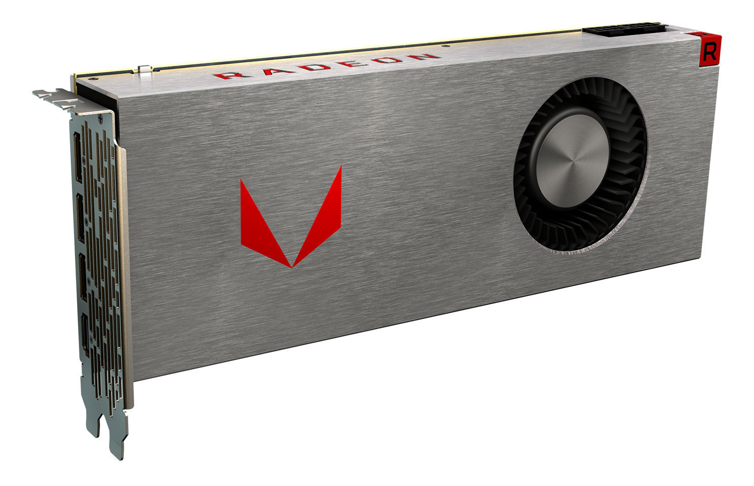
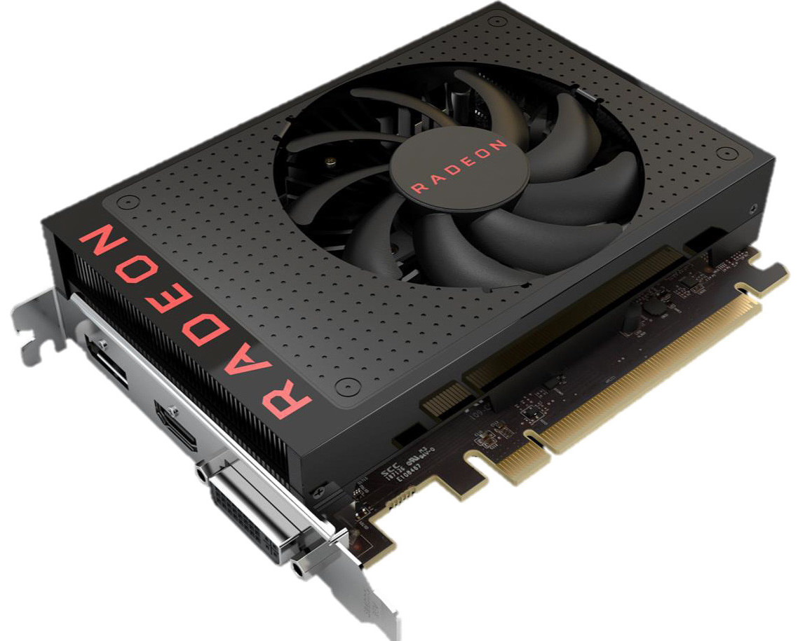
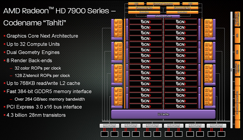
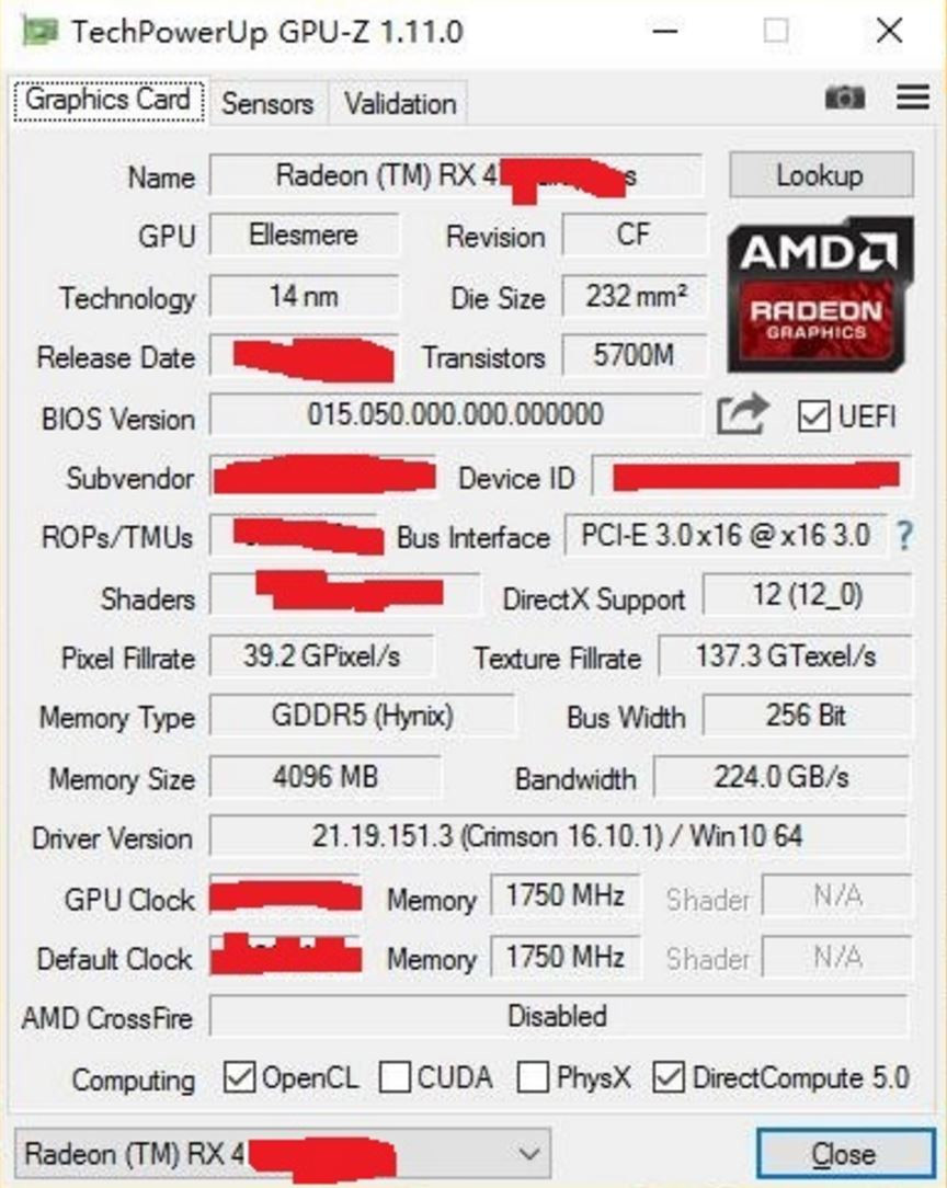
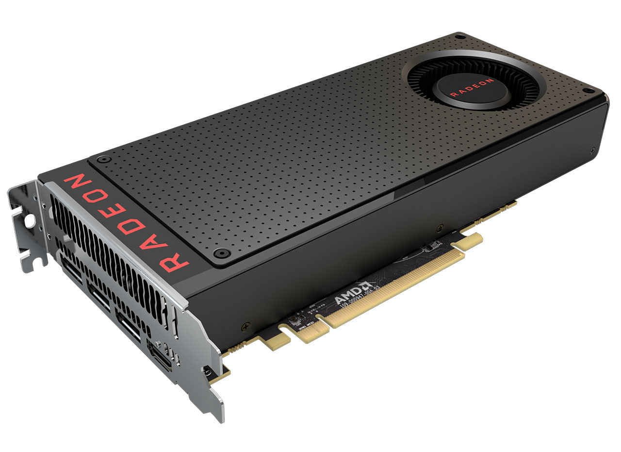
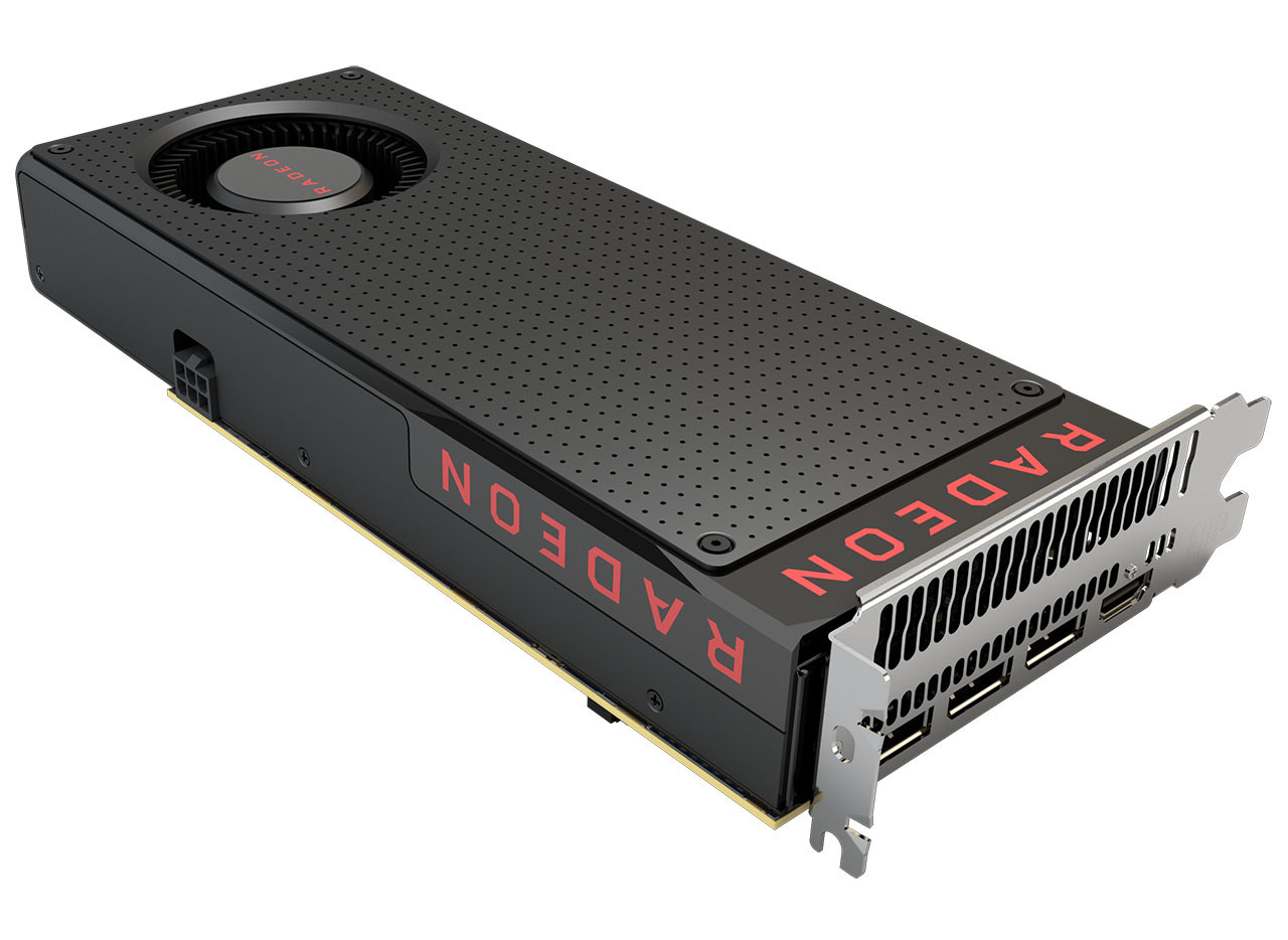
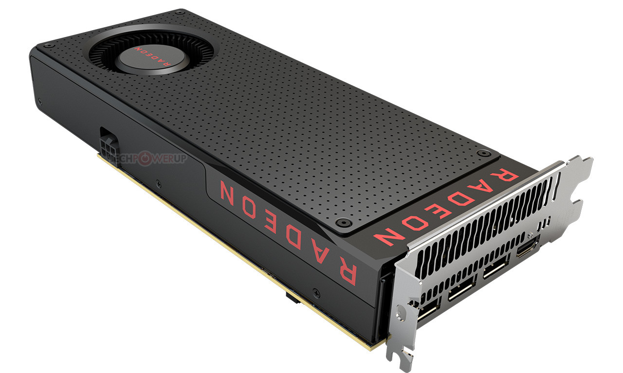
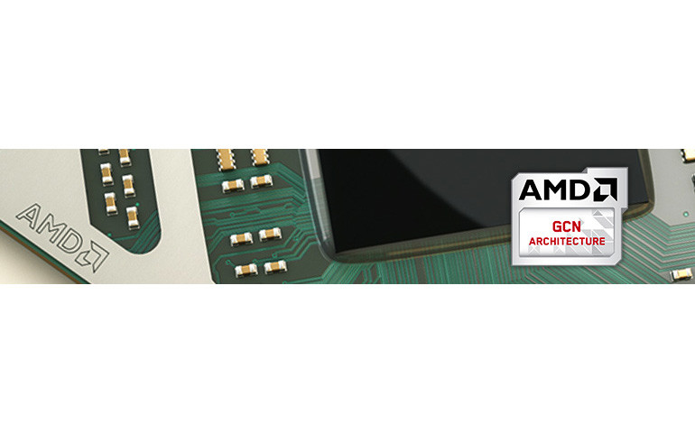
Unofficial driver packs tend to unlock features outside of a product's feature-set, and the most prominent of these for AMD Radeon GPUs is the NimeZ series. Their latest 22.7.1-based driver pack extends Radeon Noise Suppression technology support to older generation GPUs (which predate the RX 5000 series). This would cover the RX 500/400 series "Polaris," the RX Vega series, and even the much older Graphics CoreNext architecture (R# 300-series and 200-series from a decade ago). Most importantly, this brings the technology to the various generations of AMD Ryzen and A-series APUs. Use of unofficial drivers isn't covered under product warranties, but then your pre-RDNA graphics card is probably outside its coverage anyway.

AMD Releases Adrenalin 22.6.1 Legacy Software for Older GPUs

AMD today released AMD Software Adrenalin 22.6.1 Legacy. This is a special branch of AMD software designed for older GPUs based on the Graphics CoreNext architecture—Fury series, 300 series, 200 series, and HD 7000/8000 series. The driver only supports Windows 10 64-bit, there's no official support for Windows 11. Legacy branch drivers correct outstanding bugs, security vulnerabilities, and some other software-level updates, but the company doesn't advertise any new game-specific optimizations. This is probably because these GPU generations fall outside the minimum system requirements of the latest games. Still, if you'd like to reminisce with an older GPU you have lying around, or want to build a period-specific project (2010 to 2015); here's your chance. If however, you're looking for the regular Adrenalin 22.6.1 WHQL drivers for the latest GPUs, check out this page.

DOWNLOAD: AMD Software Adrenalin 22.6.1 Legacy

Ten Years in, AMD to End Support for Radeon HD 7000, R200, R300 and Fury GCN Graphics Cards

AMD is ending support for the Radeon HD 7000 series, R200 series, R300 series, and R9 Fury series graphics cards, based on the oldest versions of the Graphics CoreNext architecture. The HD 7000 series debuted in 2011, R9 200 series in 2013, with the R9 300 series essentially being rebadged. The R9 Fury series joined the ranks in 2015. This would make the Radeon 21.5.2 the final drivers from these graphics cards, giving AMD the opportunity to clean-break its drivers from the RX 400 series "Polaris" and forward. A conclusion of driver support would mean that upcoming driver releases, including the 21.6.1 drivers released today, lack support for GPUs older than the RX 400 series. Should AMD encounter glaring security flaws with its drivers, it can, in the future, release special driver updates.

AMD Radeon RX 5700 XT Confirmed to Feature 64 ROPs: Architecture Brief

AMD "Navi 10" is a very different GPU from the "Vega 10," or indeed the "Polaris 10." The GPU sees the introduction of the new RDNA graphics architecture, which is the first big graphics architecture change on an AMD GPU in nearly a decade. AMD had in 2011 released its Graphics CoreNext (GCN) architecture, and successive generations of GPUs since then, brought generational improvements to GCN, all the way up to "Vega." At the heart of RDNA is its brand new Compute Unit (CU), which AMD redesigned to increase IPC, or single-thread performance.

Before diving deeper, it's important to confirm two key specifications of the "Navi 10" GPU. The ROP count of the silicon is 64, double that of the "Polaris 10" silicon, and same as "Vega 10." The silicon has sixteen render-backends (RBs), these are quad-pumped, which work out to an ROP count of 64. AMD also confirmed that the chip has 160 TMUs. These TMUs are redesigned to feature 64-bit bi-linear filtering. The Radeon RX 5700 XT maxes out the silicon, while the RX 5700 disables four RDNA CUs, working out to 144 TMUs. The ROP count on the RX 5700 is unchanged at 64.

AMD Releases AMDVLK - Open-Source Vulkan Driver for Linux

AMD released the AMDVLK drivers for Linux. These are the first open-source AMD Radeon graphics drivers featuring 100% support for Vulkan 1.0 graphics API. The drivers include Vulkan 1.0 compliance with support for 30 Vulkan extensions, Radeon GPU Profiler support, in-built debug and profiling tools, mid-command buffer preemption, and SR-IOV virtualization support. AMDVLK implements AMD's Platform Abstraction Library (PAL), an abstraction layer that translates much of AMD's common driver code and features across platforms. The drivers support all AMD Radeon GPUs based on the Graphics CoreNext architecture, going all the way back to the Radeon HD 7000-series. The drivers are released through AMD's GPUOpen GitHub repository.

AMD Releases Radeon Software Crimson ReLive 17.8.1 WHQL Drivers

AMD released the Radeon Software Crimson ReLive Edition 17.8.1 WHQL drivers. These are the first WHQL-signed drivers to support Radeon RX Vega 64 and RX Vega 56, besides all other Graphics CoreNext based Radeon GPUs. It features optimization for "Quake Champions: Early Access" and "Agents of Mayhem." The drivers also fix stability issues with "Grand Theft Auto V," "Forza Horizon 3," and "Tekken 7." The drivers also iron out issues noted with Enhanced Sync, where online video playback is choppy. Grab the drivers from the link below.
DOWNLOAD: AMD Radeon Software Crimson ReLive 17.8.1 WHQL

The change-log follows.

NVIDIA "Pascal" Based Mining GPU Lineup Detailed

GPU-accelerated crypto-currency mining poses a threat to the consumer graphics industry, yet the revenues it brings to GPU manufacturers are hard to turn away. The more graphics cards are bought up by crypto-currency miners, the fewer there are left for gamers and the actual target-audience of graphics cards. This is particularly bad for AMD, as fewer gamers have Radeon graphics cards as opposed to miners; which means game developers no longer see AMD GPU market-share as an amorphous trigger to allocate developer resources in optimizing their games to AMD architectures.

To combat this, both AMD and NVIDIA are innovating graphics cards designed specifically for crypto-currency mining. These cards are built to a cost, lack display outputs, and have electrical and cooling mechanisms designed for 24/7 operation, even if not living up to the durability standards of real enterprise-segment graphics cards, such as Radeon Pro series or Quadro. NVIDIA's "Pascal" GPU architecture is inherently weaker than AMD's "Polaris" and older Graphics CoreNext architectures at Ethereum mining, owing in part to Pascal's lack of industry-standard asynchronous compute. This didn't deter NVIDIA from innovating a lineup of crypto-mining SKUs based on its existing "Pascal" GPUs. These include the NVIDIA P104 series based on the "GP104" silicon (on which the GTX 1080 and GTX 1070 are based); and P106 series based on the "GP106" silicon (GTX 1060 series is based on this chip). NVIDIA didn't tap into its larger "GP102" or smaller "GP107" chips, yet.

Xbox One X Hardware Specs Give Gaming Desktops a Run for their Money

Microsoft Sunday dropped its mic with the most powerful game console on paper, the Xbox One X, formerly codenamed "Project Scorpio." The bottom-line of this console is that it enables 4K Ultra HD gaming at 60 Hz. Something like this requires you to spend at least $1,200 on a gaming desktop right now. Unlike a Windows 10 PC that's been put together by various pieces of hardware, the Xbox One X is built on a closed ecosystem that's tightly controlled by Microsoft, with heavily optimized software, and a lot of secret sauce the company won't talk about. The console still puts up some mighty impressive hardware specs on paper.

To begin with, at the heart of the Xbox One X is a semi-custom SoC Microsoft co-developed with AMD, built on TSMC's 16 nm FinFET node (the same one NVIDIA builds its "Pascal" GPUs on). This chip features a GPU with almost quadruple the single-precision floating point compute power as the one which drives the Xbox One. It features 40 Graphics CoreNext (GCN) compute units (2,560 stream processors) based on one of the later versions of GCN (likely "Polaris"). The GPU is clocked at 1172 MHz. The other big component of the SoC is an eight-core CPU based on an unnamed micro-architecture evolved from "Jaguar" rather than "Bulldozer" or even "Zen." The eight cores are arranged in two quad-core units of four cores, each; with 4 MB of L2 cache. The CPU is clocked at 2.30 GHz.

Ethereum Mining Wipes Out Radeon Inventory, AMD Stock Rallies

AMD Radeon graphics cards have always been too good at GPGPU for their own good. The new Ethereum block-chain compute network, with the Ethereum crypto-currency, works really really good with AMD Radeon Graphics CoreNext architecture-based GPUs (that's every AMD GPU since Radeon HD 7000 series). As a result, not only have Ethereum prospectors bought out nearly all inventory of AMD Radeon graphics cards from the market, but also forced an inflation of used AMD Radeon graphics cards on online tech-forums, and used-goods stores on eBay and Amazon. Some of these used cards are priced higher than even launch-prices.

Every $1,000 spent on AMD Radeon hardware towards Ethereum mining is recovered within 2 months, and then as long as your hardware lasts and you're paying your power bills, you're swimming in crypto-currency that can be converted to Bitcoin and even US Dollars. One Ethereum (ETH) exchanges to USD $265 at the time of this writing. There's already $330 million worth Ethereum being traded, and that number is only going to grow as people sell USD or BTC to buy ETH and pay for entry into the Ethereum network, and use ETH as a crypto-currency.

AMD "Polaris 12" Surfaces in Linux Drivers

Apparently AMD is working on a third GPU based on its "Polaris" (4th generation Graphics CoreNext) architecture, dubbed "Polaris 12." Snooping into the code of AMDGPU DRM kernel driver, PCI-IDs 0x6980, 0x6981, 0x6985, 0x6986, 0x6987, and 0x699F, were pointing to a descriptor "Polaris 12." There are no other known specifications of this chip.

Going by convention of Polaris 11 (Radeon RX 460) being a smaller chip than Polaris 10 (RX 470, RX 480), it's likely that Polaris 12 could be an even smaller chip. On the other hand, a chip slower than Polaris 10 makes very little sense, because it would compete with "free" integrated graphics. Another possibility is that Polaris 12 is a Polaris 10 refresh on an improved process, or even made at TSMC, in which case the higher number would mean that it's a newer chip.

AMD Cripples Older GCN GPUs of Async-Compute Support?

AMD allegedly disabled asynchronous-compute technology support on older generations of Graphics CoreNext (GCN) architecture, since Radeon Software 16.9.2. With the newer drivers, "Ashes of the Singularity" no longer supports asynchronous-compute, a feature that improves performance in the game, on GPUs based on the first-generation GCN architecture, such as the Radeon R9 280X.

"Ashes of the Singularity" benchmarks run by Beyond3D forum members on GCN 1.0 hardware, comparing older drivers to version 16.9.2 shows that the game supports async-compute on the older drivers, and returns improved performance. AMD, on its part, is pointing users to a patch change-list from the developers of "Ashes..." which reads that the game supports DirectX 12 async-compute only on GCN 1.1 (eg: Radeon R9 290) and above.

AMD Releases Radeon Software Crimson Edition 16.10.3

AMD today released Radeon Software Crimson Edition 16.10.3, the month's third release of the drivers. Version 16.10.3 addresses a "Titanfall 2" intermittent game crash affecting AMD Graphics CoreNext GPUs (which is all of the GPUs under the current driver support branch). The rest of its feature-set appear to be consistent with the older Radeon Software Crimson Edition 16.10.2 drivers. Grab the drivers from the links below.
DOWNLOAD: AMD Radeon Software Crimson Edition 16.10.3 for Windows 10 64-bit | Windows 10 32-bit | Windows 8.1 64-bit | Windows 8.1 32-bit | Windows 7 64-bit | Windows 7 32-bit

AMD Readying an Answer to GeForce GTX 1050 Ti

With the arrival of the GeForce GTX 1050 Ti and GTX 1050, the sub-$150 graphics card market is beginning to heat up. AMD is finding itself with a price-performance gorge between the Radeon RX 460 and the RX 470. Citing multiple sources, VideoCardz suspects that AMD is up to something - a new Polaris 10 "Ellesmere" based SKU positioned between the RX 460 and RX 470, referred to either as the "RX 465" or the "RX 470 SE."

The new SKU is further cut down from the Polaris 10 stack, in a bid to lower TDP below the 100W mark, to around 90W. The chip features 1,792 stream processors across 28 Graphics CoreNext compute units (CUs), out of the 36 CUs physically present on the chip. The RX 470 features 32 CUs, while the RX 480 maxes out all available CUs. AMD is leaving the memory bus untouched. It features 4 GB of GDDR5 memory across a 256-bit wide memory interface, ticking at 7.00 GHz (GDDR5-effective), churning up 224 GB/s of memory bandwidth - double that of the GTX 1050 series. There's also talk of yet another SKU, with 1,536 stream processors (24/36 CUs enabled), which AMD could position against the GTX 1050 (non-Ti).

AMD Actively Promoting Vulkan Beyond GPUOpen

Vulkan, the new-generation cross-platform 3D graphics API governed by the people behind OpenGL, the Khronos Group, is gaining in relevance, with Google making it the primary 3D graphics API for Android. AMD said that it's actively promoting the API. Responding to a question by TechPowerUp in its recent Radeon Technology Group (RTG) first anniversary presser, its chief Raja Koduri agreed that the company is actively working with developers to add Vulkan to their productions, and optimize them for Radeon GPUs. This, we believe, could be due to one of many strategic reasons.

First, Vulkan works inherently better on AMD Graphics CoreNext GPU architecture because it's been largely derived from Mantle, a now defunct 3D graphics API by AMD that brings a lot of "close-to-metal" API features that make game consoles more performance-efficient, over to the PC ecosystem. The proof of this pudding is the AAA title and 2016 reboot of the iconic first-person shooter "Doom," in which Radeon GPUs get significant performance boosts switching from the default OpenGL renderer to Vulkan. These boosts aren't as pronounced on NVIDIA GPUs.

AMD Unveils its 7th Generation A-Series Desktop APUs

AMD today unveiled its 7th generation A-series desktop APUs. Unlike its predecessors, the new chips are full-fledged SoCs, built in the new socket AM4 package, on which the company plans to launch its "Zen" processors. The 7th gen A-series APUs are based on the "Bristol Ridge" silicon, and are the first fully-integrated SoCs (systems-on-chip) from the company in the performance-desktop segment, in that the APU completely integrates the functionality of a motherboard chipset, including its FCH or southbridge.

This level of integration includes PCI-Express root-complex, USB 3.0, and storage interfaces such as SATA 6 Gb/s emerging directly from the AM4 socket. Some AM4 motherboards could still include a sort of "chipset," which expands connectivity options, such as USB 3.1 ports, additional SATA ports, and a few more downstream PCI-Express lanes. The amount of downstream connectivity and features decide the grade of the chipset. AMD is initially launching two chipsets, the A320 for the entry-level segment, and the B350 for mainstream desktops. The company plans to launch an even more feature-rich chipset at a later date (probably alongside ZEN "Summit Ridge" CPUs).

AMD Radeon RX 480 Graphics Card Now Available

AMD today announced availability of its Radeon RX 480 graphics card. The card is currently only available in its 8 GB variant, with the more cost-effective 4 GB variant touting the magic price-tag of $199 slated for July. The 8 GB variant being launched today will start at $229. Based on the 14 nanometer Polaris 10 silicon, the RX 480 takes advantage of the 4th generation Graphics CoreNext (GCN) architecture.

The chip features 2,304 stream processors spread across 36 GCN compute units, 144 TMUs, 32 ROPs, and a 256-bit GDDR5 memory interface, holding 8 GB of memory. At its given clock speeds, the card features 256 GB/s of memory bandwidth, although AMD claims DCC memory compression technology to effectively increase memory bandwidth by up to 30 percent in the best case scenarios. The core ticks at 1266 MHz, and the memory at 8 GHz (GDDR5-effective). The card features a TDP of just 150W, and draws power from a single 6-pin PCIe power connector. Display outputs include three DisplayPort 1.4 and one HDMI 2.0b. Custom-design cards could feature DVI connectors.

Read the TechPowerUp Reviews of this card: AMD Radeon RX 480 8GB | AMD Radeon RX 480 CrossFire

AMD "Vega 10" GPU Crosses a Development Milestone

AMD Radeon Technologies Group (RTG) chief Raja Koduri was in Shanghai last week to meet with one of the design teams of the "Polaris10" and the upcoming "Vega10." He tweeted that development of "Vega10" had just crossed a milestone, although it's a long way to go before you can see it. The 5th generation Graphics CoreNext architecture, and successor to the upcoming "Polaris" architecture, "Vega" promises a higher performance/Watt than "Polaris," which in turn boasts of a large energy efficiency leap over its predecessor.

One of the most notable derivatives of "Vega" is the "Vega10," poised to be a performance-segment GPU, which will make it to the market alongside "Vega11," a larger enthusiast-segment chip. The Vega10 is rumored to feature 4,096 stream processors spread across 64 compute units, and is expected to be a competitor to NVIDIA's GP104 silicon. The larger Vega11 could compete with larger chips based on the "Pascal" architecture, such as the GP102.

AMD Radeon RX 480 "Polaris" Launched at $199

AMD made a bold move in launching its first "Polaris" architecture based performance-segment GPU, the Radeon RX 480 at a starting price of US $199. The company claims that it will perform on-par with $500 graphics cards from the previous generation, directly hinting at performance being on par with the Radeon R9 Fury and R9 Nano. Although it's not in the league of the GTX 1070 or the GTX 1080, this level of performance at $199 could certainly disrupt things for NVIDIA, as it presents an attractive option for people still gaming on 1440p and 1080p resolutions (the overwhelming majority). The R9 Fury can handle any game at 1440p.

The Radeon RX 480 is based on the 14 nm "Ellesmere" silicon, fabbed by GlobalFoundries. It's publicly known that GloFlo has a 14 nm fab in Malta (upstate New York), USA. The RX 480 is based on AMD's 4th generation Graphics CoreNext architecture, codenamed "Polaris." It features 2,304 stream processors, spread across 36 compute units (CUs). Its single-precision floating point performance is rated by AMD to be "greater than 5 TFLOP/s." The chip features a 256-bit wide GDDR5 memory interface, with memory clocked at 8 Gbps, yielding memory bandwidth of 256 GB/s. There will be two variants of this card, 4 GB and 8 GB. It's the 4 GB variant that starts at $199, the 8 GB variant is expected to be priced at $229. AMD confirmed that the GPU will support DisplayPort 1.4 although it's certified up to DisplayPort 1.3. The typical board power is rated at 150W. The card could be available from 29th June.

More Polaris10 and Polaris11 Specifications Revealed

Industry sources revealed to TechPowerUp some pretty interesting specifications of AMD's two upcoming GPUs based on the 4th generation Graphics CoreNext "Polaris" architecture. The company is preparing a performance-segment GPU and a mainstream one. It turns out, that the performance-segment chip, which the press has been referring to as "Ellesmere," could feature 32 compute units (CUs), and not the previously thought 40.

Assuming that each CU continues to consist of 64 stream processors (SP), you're looking at an SP count of 2,048. What's more, this chip is said to offer a single-precision floating point performance of 5.5 TFLOP/s, as claimed by AMD. To put this into perspective, the company had claimed 5.2 TFLOP/s for the "Hawaii"/"Grenada" based FirePro W9100, which launched earlier this February, and that SKU featured all 2,816 SP present on the chip. So this chip is definitely faster than most "Hawaii" based SKUs.

AMD Teases Polaris 10 and Polaris 11 ASIC Images

AMD posted a new webpage for its upcoming "Polaris" GPU architecture, outlining its various innovations - 4th gen. Graphics CoreNext, 4K H.265 60 Hz game-streaming, next-generation display engine with support for DisplayPort 1.3 and HDMI 2.0, XConnect Technology, and the foundation of GPUOpen. In this page, the company inadvertently leaked pictures of its upcoming Polaris 10 "Ellesmere" and Polaris 11 "Baffin" ASICs.

The mast image of the page has a faded 3-quarter shot of a "small" GPU with a die that's almost 30% of the package area. This hints at Polaris 11 "Baffin." This chip is rumored to feature a 128-bit GDDR5/GDDR5X memory interface, and so its pin-count, and conversely, package-size is less. Then in its "4th gen GCN" heading image, AMD showed a picture of a bigger GPU. At first glance, you could assume that it's either "Tonga XT" or "Tahiti" looking at its support brace, but VideoCardz observed that the on-package electrical components in this image are arranged nothing like on the "Tonga" or "Tahiti." This could very well be Polaris 10 "Ellesmere."

PlayStation 4K to Feature a 2,304-SP AMD "Polaris" GPU

Sony's upcoming 4K Ultra HD game console, which its fans are referring to as the "PlayStation 4K," while being internally referred to by Sony as "NEO," could feature a very powerful GPU. AMD could custom-design the SoC that drives the console, to feature an 8-core 64-bit x86 CPU based on the "Jaguar" micro-architecture, running at 2.10 GHz; and a GPU component featuring 36 compute units based on "next-generation Graphics CoreNext" architecture.

36 next-gen GCN compute units sounds an awful lot like the specs of the Polaris10 "Ellesmere" chip in its Radeon R9 480 configuration, working out to a stream processor count of 2,304 - double that of the 1,152 on the current-gen PlayStation 4. The SoC is also rumored to feature a 256-bit GDDR5 memory interface holding 8 GB of memory. This memory will be used as both system and video memory, just like on the current-gen PlayStation 4. The memory bandwidth will be increased to 218 GB/s from the current 176 GB/s. Besides 4K Ultra HD gaming, this chip could also prepare Sony for VR headsets, leveraging AMD's LiquidVR tech.

AMD to Launch Radeon R7 470 and R9 480 at Computex

Computex 2016 could see some major consumer graphics action, with AMD reportedly planning to launch two mid-thru-performance segment products on the sidelines of the event - the Radeon R7 470, based on the 14 nm "Baffin" (Polaris 11) silicon, and the Radeon R9 480, based on the 14 nm "Ellesmere" (Polaris 10) silicon. The R7 470 could succeed the R7 370 series in not just performance, but also offer a leap in energy efficiency, with a TDP of less than 50W. The R9 480, on the other hand, could feature a TDP of just 110-135W (R9 380 is rated at 190W).

The R9 480, based on the "Ellesmere" (Polaris 10) is shaping up to be a particularly interesting silicon. It's rumored to feature 2,304 stream processors based on the 4th generation Graphics CoreNext architecture, with 2,560 stream processors being physically present on the chip; and a 256-bit wide GDDR5 (GDDR5X-ready) memory controller. 8 GB could be the standard memory amount. AMD could keep the clock speeds relatively low, with 800-1050 MHz GPU clocks. Imagine R9 390-like performance at half its power-draw.

Upcoming AMD "Polaris" and "Vega" GPU Compute Unit Counts Surface

AMD's upcoming GPUs based on the "Polaris" and "Vega" architectures appear to be taking advantage of performance/Watt gains to keep stream processor counts low, and chips small, according to a VideoCardz analysis of curious-looking CompuBench entries. Assuming that a Graphics CoreNext (GCN) compute unit (CU) of the "Polaris" architecture, like the three versions of GCN before it, consists of 64 stream processors, AMD's Polaris 11 silicon, codenamed "Baffin," could feature over 1,024 stream processors, across 16 CUs; Polaris 10, codenamed "Ellesmere," could feature over 2,304 stream processors spread across over 36 CUs; and Vega 10 featuring 4,096 stream processors, spread across 64 CUs.

The "Baffin" silicon succeeds current generation "Curacao" silicon, driving mid-range graphics cards. It is expected to feature a 128-bit wide GDDR5 memory interface, holding 4 GB of memory. The "Ellesmere" silicon succeeds current-generation "Tonga" silicon, driving performance-segment SKUs. It could feature up to 8 GB of GDDR5(X) memory. These two chips could see the light of the day by mid-2016. The third chip out of AMD's stable, Vega 10, could succeed "Fiji," overcoming its biggest marketing shortcoming - 4 GB memory. Taking advantage of HBM2 interface, it could feature 16 GB of memory. It could launch some time in early-2017. AMD is claiming a massive 2.5X performance-per-Watt increase for "Polaris" over the current GCN 1.2 architecture, which drives the "Tonga" and "Fiji" chips, and so these stream processor counts could look deceptively insufficient.

AMD Outs "Bristol Ridge" APU Performance Numbers

Although AMD's upcoming socket AM4 heralds new lines of processors and APUs based on the company's next-generation "Zen" CPU micro-architecture, some of the first APUs will continue to be based the current "Excavator" architecture. The "Bristol Ridge" is one such chip. It made its mobile debut as the 7th generation A-Series and FX-Series mobile APUs, and is en route to the desktop platform, in the AM4 package. What sets the AM4 package apart from the FM2+ package, and in turn "Bristol Ridge" from "Carrizo" is that the platform integrates even the southbridge (FCH) into the APU die. This could explain the 1,331-pin count of the AM4 socket.

The "Bristol Ridge" silicon is likely built on the existing 28 nm process. That's not the only thing "current-gen" about this chip. Its CPU component consists of two "Excavator" modules that make up four CPU cores, with 4 MB total cache; and its integrated GPU will likely be based on the Graphics CoreNext 1.2 "Volcanic Islands" architecture, the same one which drives the "Tonga" and "Fiji" discrete GPUs. The integrated memory controller supports dual-channel DDR4 memory. In its performance benchmarks, an AM4 APU based on the "Bristol Ridge" silicon was pitted against older 6th generation APUs, in which it was found to be as much as 23 percent faster.

AMD "Greenland" Vega10 Silicon Features 4096 Stream Processors?

The LinkedIn profile of an R&D manager at AMD discloses key details of the company's upcoming "Greenland" graphics processor, which is also codenamed Vega10. Slated for an early-2017 launch, according to AMD's GPU architecture roadmap, "Greenland" will be built on AMD's "Vega" GPU architecture, which succeeds even the "Polaris" architecture, which is slated for later this year.

The LinkedIn profile of Yu Zheng, an R&D manager at AMD (now redacted), screencaptured by 3DCenter.org, reveals the "shader processor" (stream processor) count of Vega10 to be 4,096. This may look identical to the SP count of "Fiji," but one must take into account "Greenland" being two generations of Graphics CoreNext tech ahead of "Fiji," and that the roadmap slide hints at HBM2 memory, which could be faster. One must take into account AMD's claims of a 2.5X leap in performance-per-Watt over the current architecture with Polaris, so Vega could only be even faster.
Return to Keyword Browsing
Apr 18th, 2024 00:52 EDT change timezone

New Forum Posts

Popular Reviews

Controversial News Posts