News Posts matching #TSMC

Return to Keyword Browsing

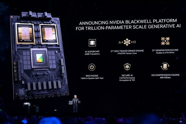
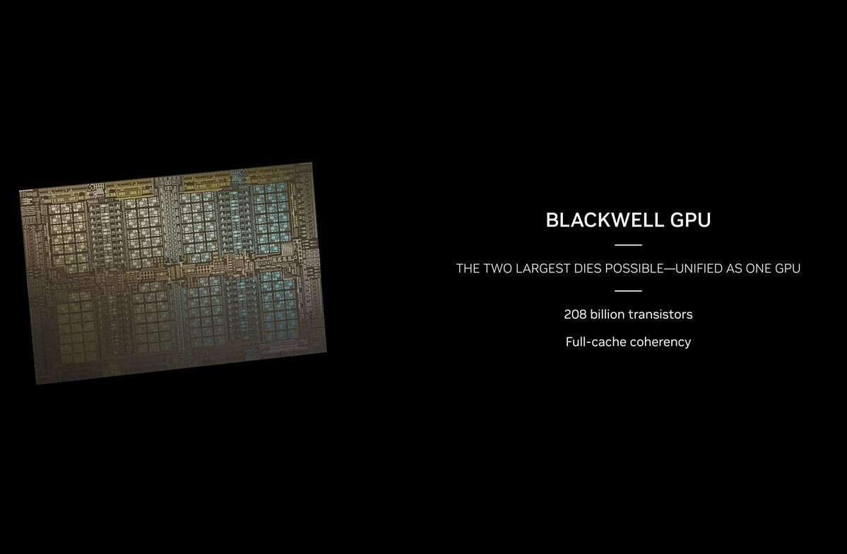
SK hynix Collaborates with TSMC on HBM4 Chip Packaging

SK hynix Inc. announced today that it has recently signed a memorandum of understanding with TSMC for collaboration to produce next-generation HBM and enhance logic and HBM integration through advanced packaging technology. The company plans to proceed with the development of HBM4, or the sixth generation of the HBM family, slated to be mass-produced from 2026, through this initiative.

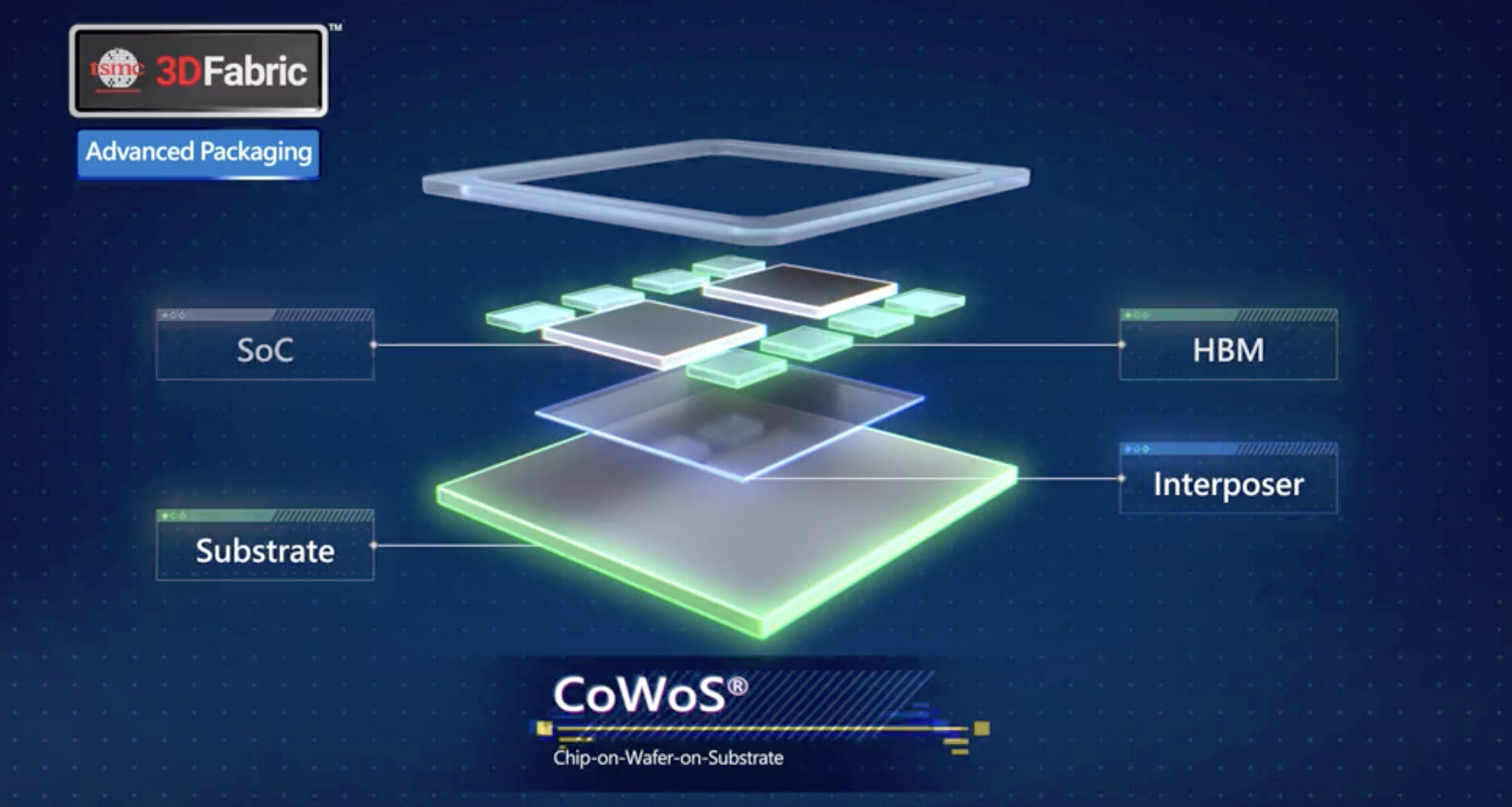
SK hynix said the collaboration between the global leader in the AI memory space and TSMC, a top global logic foundry, will lead to more innovations in HBM technology. The collaboration is also expected to enable breakthroughs in memory performance through trilateral collaboration between product design, foundry, and memory provider. The two companies will first focus on improving the performance of the base die that is mounted at the very bottom of the HBM package. HBM is made by stacking a core DRAM die on top of a base die that features TSV technology, and vertically connecting a fixed number of layers in the DRAM stack to the core die with TSV into an HBM package. The base die located at the bottom is connected to the GPU, which controls the HBM.

Demand for NVIDIA's Blackwell Platform Expected to Boost TSMC's CoWoS Total Capacity by Over 150% in 2024

NVIDIA's next-gen Blackwell platform, which includes B-series GPUs and integrates NVIDIA's own Grace Arm CPU in models such as the GB200, represents a significant development. TrendForce points out that the GB200 and its predecessor, the GH200, both feature a combined CPU+GPU solution, primarily equipped with the NVIDIA Grace CPU and H200 GPU. However, the GH200 accounted for only approximately 5% of NVIDIA's high-end GPU shipments. The supply chain has high expectations for the GB200, with projections suggesting that its shipments could exceed millions of units by 2025, potentially making up nearly 40 to 50% of NVIDIA's high-end GPU market.

Although NVIDIA plans to launch products such as the GB200 and B100 in the second half of this year, upstream wafer packaging will need to adopt more complex and high-precision CoWoS-L technology, making the validation and testing process time-consuming. Additionally, more time will be required to optimize the B-series for AI server systems in aspects such as network communication and cooling performance. It is anticipated that the GB200 and B100 products will not see significant production volumes until 4Q24 or 1Q25.

Meta Announces New MTIA AI Accelerator with Improved Performance to Ease NVIDIA's Grip

Meta has announced the next generation of its Meta Training and Inference Accelerator (MTIA) chip, which is designed to train and infer AI models at scale. The newest MTIA chip is a second-generation design of Meta's custom silicon for AI, and it is being built on TSMC's 5 nm technology. Running at the frequency of 1.35 GHz, the new chip is getting a boost to 90 Watts of TDP per package compared to just 25 Watts for the first-generation design. Basic Linear Algebra Subprograms (BLAS) processing is where the chip shines, and it includes matrix multiplication and vector/SIMD processing. At GEMM matrix processing, each chip can process 708 TeraFLOPS at INT8 (presumably meant FP8 in the spec) with sparsity, 354 TeraFLOPS without, 354 TeraFLOPS at FP16/BF16 with sparsity, and 177 TeraFLOPS without.

Classical vector and processing is a bit slower at 11.06 TeraFLOPS at INT8 (FP8), 5.53 TeraFLOPS at FP16/BF16, and 2.76 TFLOPS single-precision FP32. The MTIA chip is specifically designed to run AI training and inference on Meta's PyTorch AI framework, with an open-source Triton backend that produces compiler code for optimal performance. Meta uses this for all its Llama models, and with Llama3 just around the corner, it could be trained on these chips. To package it into a system, Meta puts two of these chips onto a board and pairs them with 128 GB of LPDDR5 memory. The board is connected via PCIe Gen 5 to a system where 12 boards are stacked densely. This process is repeated six times in a single rack for 72 boards and 144 chips in a single rack for a total of 101.95 PetaFLOPS, assuming linear scaling at INT8 (FP8) precision. Of course, linear scaling is not quite possible in scale-out systems, which could bring it down to under 100 PetaFLOPS per rack.
Below, you can see images of the chip floorplan, specifications compared to the prior version, as well as the system.

Intel Launches Gaudi 3 AI Accelerator: 70% Faster Training, 50% Faster Inference Compared to NVIDIA H100, Promises Better Efficiency Too

During the Vision 2024 event, Intel announced its latest Gaudi 3 AI accelerator, promising significant improvements over its predecessor. Intel claims the Gaudi 3 offers up to 70% improvement in training performance, 50% better inference, and 40% better efficiency than Nvidia's H100 processors. The new AI accelerator is presented as a PCIe Gen 5 dual-slot add-in card with a 600 W TDP or an OAM module with 900 W. The PCIe card has the same peak 1,835 TeraFLOPS of FP8 performance as the OAM module despite a 300 W lower TDP. The PCIe version works as a group of four per system, while the OAM HL-325L modules can be run in an eight-accelerator configuration per server. This likely will result in a lower sustained performance, given the lower TDP, but it confirms that the same silicon is used, just finetuned with a lower frequency. Built on TSMC's N5 5 nm node, the AI accelerator features 64 Tensor Cores, delivering double the FP8 and quadruple FP16 performance over the previous generation Gaudi 2.

The Gaudi 3 AI chip comes with 128 GB of HBM2E with 3.7 TB/s of bandwidth and 24 200 Gbps Ethernet NICs, with dual 400 Gbps NICs used for scale-out. All of that is laid out on 10 tiles that make up the Gaudi 3 accelerator, which you can see pictured below. There is 96 MB of SRAM split between two compute tiles, which acts as a low-level cache that bridges data communication between Tensor Cores and HBM memory. Intel also announced support for the new performance-boosting standardized MXFP4 data format and is developing an AI NIC ASIC for Ultra Ethernet Consortium-compliant networking. The Gaudi 3 supports clusters of up to 8192 cards, coming from 1024 nodes comprised of systems with eight accelerators. It is on track for volume production in Q3, offering a cost-effective alternative to NVIDIA accelerators with the additional promise of a more open ecosystem. More information and a deeper dive can be found in the Gaudi 3 Whitepaper.

US Backs TSMC's $65B Arizona Investment with $11.6B Support Package

According to the latest report from Bloomberg, the US government under Joe Biden's administration has announced plans to provide Taiwan Semiconductor Manufacturing Company (TSMC) with a substantial financial support package worth $11.6 billion. The package is composed of $6.6 billion in grants and up to $5 billion in loans. This represents the most significant financial assistance approved under the CHIPS and Science Act, a key initiative to resurrect the US chip industry. The funding will aid TSMC in establishing three cutting-edge semiconductor production facilities in Arizona, with the company's total investment in the state expected to exceed an impressive $65 billion. TSMC's multi-phase Arizona project will commence with the construction of a fab module near its existing Fab 21 facility. Production using 4 nm and 5 nm process nodes is slated to begin by early 2025. The second phase, scheduled for 2028, will focus on even more advanced 2 nm and 3 nm technologies.

TSMC has kept details about the third facility's production timeline and process node under wraps. The company's massive investment in Arizona is expected to profoundly impact the local economy, creating 6,000 high-tech manufacturing jobs and over 20,000 construction positions. Moreover, $50 million has been earmarked for training local workers, which aligns with President Joe Biden's goal of bolstering domestic manufacturing and technological independence. However, TSMC's Arizona projects have encountered obstacles, including labor disputes and uncertainties regarding government support, resulting in delays for the second facility's production timeline. Additionally, reports suggest that at least one TSMC supplier has abandoned plans to set up operations in Arizona due to workforce-related challenges.

Magnitude 7.4 Earthquake in Taiwan Halts Production at TSMC and Other Foundries

At 07:58 local time, Taiwan was rocked by a magnitude 7.4 earthquake on the east coast which was felt nationwide and as far as to the southeastern parts of China and southern Japan. It caused some major damage in the east coast city of Hualien where the epicentre of the quake was located, as well as surrounding areas. The earthquake reportedly left nine people dead and over 900 people injured islandwide. TSMC, UMC, PSMC and Innolux all halted some of their production lines in the Hsinchu Science Park on the west coast of the island, although this is said to have been as a preventive step, rather than caused by actual damage from the earthquake.

All the above-mentioned companies also evacuated their staff from their factories due to the intensity of the quake, as it reached a magnitude of around four or five almost island wide. The semiconductor manufacturers are all inspecting their fabs now to make sure none of the equipment was damaged by the earthquake. Innolux also has a factory in the southern city of Kaohsiung and has reported that it has suspended production in Hsinchu, but that production in Kaohsiung wasn't affected. Local media in Taiwan hasn't made any mention of the likes of Micron or other chip manufacturers, but it's likely that the situation is similar, since all of these companies are located in the same areas on the island. Aftershocks have continued throughout the day and there's a risk for further big earthquakes to follow in the coming days.
Images courtesy of the Taiwan Central Weather Administration (CWA).

Update 15:11 UTC: Updated with an official statement from Micron below.

Apple M3 Ultra Chip Could be a Monolithic Design Without UltraFusion Interconnect

As we witness Apple's generational updates of the M series of chips, the highly anticipated SKU of the 3rd generation of Apple M series yet-to-be-announced top-of-the-line M3 Ultra chip is growing speculations from industry insiders. The latest round of reports suggests that the M3 Ultra might step away from its predecessor's design, potentially adopting a monolithic architecture without the UltraFusion interconnect technology. In the past, Apple has relied on a dual-chip design for its Ultra variants, using the UltraFusion interconnect to combine two M series Max chips. For example, the second generation M Ultra chip, M2 Ultra, boasts 134 billion transistors across two 510 mm² chips. However, die-shots of the M3 Max have sparked discussions about the absence of dedicated chip space for the UltraFusion interconnect.

While the absence of visible interconnect space on early die-shots is not conclusive evidence, as seen with the M1 Max not having visible UltraFusion interconnect and still being a part of M1 Ultra with UltraFusion, industry has led the speculation that the M3 Ultra may indeed feature a monolithic design. Considering that the M3 Max has 92 billion transistors and is estimated to have a die size between 600 and 700 mm², going Ultra with these chips may be pushing the manufacturing limit. Considering the maximum die size limit of 848 mm² for the TSMC N3B process used by Apple, there may not be sufficient space for a dual-chip M3 Ultra design. The potential shift to a monolithic design for the M3 Ultra raises questions about how Apple will scale the chip's performance without the UltraFusion interconnect. Competing solutions, such as NVIDIA's Blackwell GPU, use a high-bandwidth C2C interface to connect two 104 billion transistor chips, achieving a bandwidth of 10 TB/s. In comparison, the M2 Ultra's UltraFusion interconnect provided a bandwidth of 2.5 TB/s.

Intel Lunar Lake Chiplet Arrangement Sees Fewer Tiles—Compute and SoC

Intel Core Ultra "Lunar Lake-MX" will be the company's bulwark against Apple's M-series Pro and Max chips, designed to power the next crop of performance ultraportables. The MX codename extension denotes MoP (memory-on-package), which sees stacked LPDDR5X memory chips share the package's fiberglass substrate with the chip, to conserve PCB footprint, and give Intel greater control over the right kind of memory speed, timings, and power-management features suited to its microarchitecture. This is essentially what Apple does with its M-series SoCs powering its MacBooks and iPad Pros. Igor's Lab scored the motherlode on the way Intel has restructured the various components across its chiplets, and the various I/O wired to the package.

When compared to "Meteor Lake," the "Lunar Lake" microarchitecture sees a small amount of "re-aggregation" of the various logic-heavy components of the processor. On "Meteor Lake," the CPU cores and the iGPU sat on separate tiles—Compute tile and Graphics tile, respectively, with a large SoC tile sitting between them, and a smaller I/O tile that serves as an extension of the SoC tile. All four tiles sat on top of a Foveros base tile, which is essentially an interposer—a silicon die that facilitates high-density microscopic wiring between the various tiles that are placed on top of it. With "Lunar Lake," there are only two tiles—the Compute tile, and the SoC tile.

TSMC 3nm Node to Make 20% of Company's Revenues in 2024

The 3 nm EUV node, which will be TSMC's final semiconductor fabrication node to implement FinFET transistors, will make for a staggering 20% of TSMC's revenues in 2024, a report by ICSmart says. 20% is big for a new foundry node, considering that TSMC is simultaneously running 4 nm and 5 nm EUV nodes; 6 nm and 7 nm DUV nodes; and several older mature nodes. Apple is expected to be the foundry's biggest customer for 3 nm, as it could power the company's current A17 and M3, and upcoming A18 and M4 line of chips for its next-generation iPhone and MacBooks; followed by NVIDIA, AMD, and possibly even Intel. AMD is expected to build some versions of its upcoming "Zen 5" processors on 3 nm; while Intel is expected to use 3 nm for some of the tiles of its upcoming "Lunar Lake" processor. The same report goes to suggest that 3 nm will make up 30% of TSMC's revenues in 2025.

Nvidia CEO Reiterates Solid Partnership with TSMC

One key takeaway from the ongoing GTC is that Nvidia's AI empire has taken shape with strong partnerships from TSMC and other Taiwanese makers, such as those major server ODMs.

According to the news report from the technology-focused media DIGITIMES Asia, during his keynote at GTC on March 18, Huang underscored his company's partnerships with TSMC, as well as the supply chain in Taiwan. Speaking to the press later, Huang said Nvidia will have a very strong demand for CoWoS, the advanced packaging services TSMC offers.

MediaTek Licenses NVIDIA GPU IP for AI-Enhanced Vehicle Processors

NVIDIA has been offering its GPU IP for more than a decade now ever since the introduction of Kepler uArch, and its IP has had relatively low traction in other SoCs. However, that trend seems to be reaching an inflection point as NVIDIA has given MediaTek a license to use its GPU IP to produce the next generation of processors for the auto industry. The newest MediaTek Dimensity Auto Cockpit family consists of CX-1, CY-1, CM-1, and CV-1, where the CX-1 targets premium vehicles, CM targets medium range, and CV targets lower-end vehicles, probably divided by their compute capabilities. The Dimensity Auto Cockpit family is brimming with the latest technology, as the processor core of choice is an Armv9-based design paired with "next-generation" NVIDIA GPU IP, possibly referring to Blackwell, capable of doing ray tracing and DLSS 3, powered by RTX and DLA.

The SoC is supposed to integrate a lot of technology to lower BOM costs of auto manufacturing, and it includes silicon for controlling displays, cameras (advanced HDR ISP), audio streams (multiple audio DSPs), and connectivity (WiFi networking). Interestingly, the SKUs can play movies with AI-enhanced video and support AAA gaming. MediaTek touts the Dimensity Auto Cockpit family with fully local AI processing capabilities, without requiring assistance from outside servers via WiFi, and 3D spatial sensing with driver and occupant monitoring, gaze-aware UI, and natural controls. All of that fits into an SoC fabricated at TSMC's fab on a 3 nm process and runs on the industry-established NVIDIA DRIVE OS.

NVIDIA "Blackwell" GeForce RTX to Feature Same 5nm-based TSMC 4N Foundry Node as GB100 AI GPU

Following Monday's blockbuster announcements of the "Blackwell" architecture and NVIDIA's B100, B200, and GB200 AI GPUs, all eyes are now on its client graphics derivatives, or the GeForce RTX GPUs that implement "Blackwell" as a graphics architecture. Leading the effort will be the new GB202 ASIC, a successor to the AD102 powering the current RTX 4090. This will be NVIDIA's biggest GPU with raster graphics and ray tracing capabilities. The GB202 is rumored to be followed by the GB203 in the premium segment, the GB205 a notch lower, and the GB206 further down the stack. Kopite7kimi, a reliable source with NVIDIA leaks, says that the GB202 silicon will be built on the same TSMC 4N foundry node as the GB100.

TSMC 4N is a derivative of the company's mainline N4P node, the "N" in 4N stands for NVIDIA. This is a nodelet that TSMC designed with optimization for NVIDIA SoCs. TSMC still considers the 4N as a derivative of the 5 nm EUV node. There is very little public information on the power- and transistor density improvements of the TSMC 4N over TSMC N5. For reference, the N4P, which TSMC regards as a 5 nm derivative, offers a 6% transistor-density improvement, and a 22% power efficiency improvement. In related news, Kopite7kimi says that with "Blackwell," NVIDIA is focusing on enlarging the L1 caches of the streaming multiprocessors (SM), which suggests a design focus on increasing the performance at an SM-level.

Unwrapping the NVIDIA B200 and GB200 AI GPU Announcements

NVIDIA on Monday, at the 2024 GTC conference, unveiled the "Blackwell" B200 and GB200 AI GPUs. These are designed to offer an incredible 5X the AI inferencing performance gain over the current-gen "Hopper" H100, and come with four times the on-package memory. The B200 "Blackwell" is the largest chip physically possible using existing foundry tech, according to its makers. The chip is an astonishing 208 billion transistors, and is made up of two chiplets, which by themselves are the largest possible chips.

Each chiplet is built on the TSMC N4P foundry node, which is the most advanced 4 nm-class node by the Taiwanese foundry. Each chiplet has 104 billion transistors. The two chiplets have a high degree of connectivity with each other, thanks to a 10 TB/s custom interconnect. This is enough bandwidth and latency for the two to maintain cache coherency (i.e. address each other's memory as if they're their own). Each of the two "Blackwell" chiplets has a 4096-bit memory bus, and is wired to 96 GB of HBM3E spread across four 24 GB stacks; which totals to 192 GB for the B200 package. The GPU has a staggering 8 TB/s of memory bandwidth on tap. The B200 package features a 1.8 TB/s NVLink interface for host connectivity, and connectivity to another B200 chip.

TSMC and Synopsys Bring Breakthrough NVIDIA Computational Lithography Platform to Production

NVIDIA today announced that TSMC and Synopsys are going into production with NVIDIA's computational lithography platform to accelerate manufacturing and push the limits of physics for the next generation of advanced semiconductor chips. TSMC, the world's leading foundry, and Synopsys, the leader in silicon to systems design solutions, have integrated NVIDIA cuLitho with their software, manufacturing processes and systems to speed chip fabrication, and in the future support the latest-generation NVIDIA Blackwell architecture GPUs.

"Computational lithography is a cornerstone of chip manufacturing," said Jensen Huang, founder and CEO of NVIDIA. "Our work on cuLitho, in partnership with TSMC and Synopsys, applies accelerated computing and generative AI to open new frontiers for semiconductor scaling." NVIDIA also introduced new generative AI algorithms that enhance cuLitho, a library for GPU-accelerated computational lithography, dramatically improving the semiconductor manufacturing process over current CPU-based methods.

TSMC Reportedly Investing $16 Billion into New CoWoS Facilities

TSMC is experiencing unprecedented demand from AI chip customers—unnamed parties have (fancifully) requested the construction of entirely new fabrication facilities. Taiwan's leading semiconductor contract manufacturer seems to concentrating on "sensible" expansions, mainly in the area of CoWoS packaging output—according to an Economic Daily report, company leadership and local government were negotiating over the construction of four new advanced packaging plants. Insiders propose that plans have been revised—an investment in excess of 500 billion yuan ($16 billion) will enable the founding of six new CoWoS-focused facilities. TSMC is expected to make an official announcement next month—industry moles reckon that construction work will start in April. Two (of the six total) advanced packaging plants could become fully operational before the conclusion of 2024.

Lately, TSMC has initiated an ambitious recruitment drive—targeting around 6000 new workers. A touring entity is tasked with the attraction of "talents with high enthusiasm for semiconductors." The majority of new recruits are likely heading to new or expanded Taiwan-based facilities. The Economic Daily report proposes that Chiayi City's technological hub will play host to TSMC's new CoWoS packaging plants. A DigiTimes Asia news piece (from January) posited that TSMC leadership anticipates CoWoS output reaching 44,000 units by the end of 2024. This predicted tally could grow, thanks to the (rumored) activation of additional factories. CoWoS packaging is considered to be a vital aspect of AI accelerators—insiders believe that TSMC's latest investment will boost production of NVIDIA H100 GPUs. The combined output of six new CoWoS plants will assist greatly in the creation of next-gen B100 chips.

NVIDIA B100 "Blackwell" AI GPU Technical Details Leak Out

Jensen Huang's opening GTC 2024 keynote is scheduled to happen tomorrow afternoon (13:00 Pacific time)—many industry experts believe that the NVIDIA boss will take the stage and formally introduce his company's B100 "Blackwell" GPU architecture. An enlightened few have been treated to preview (AI and HPC) units—including Dell's CEO, Jeff Clarke—but pre-introduction leaks have not flowed out. Team Green is likely enforcing strict conditions upon a fortunate selection of trusted evaluators, within a pool of ecosystem partners and customers.

Today, a brave soul has broken that silence—tech tipster, AGF/XpeaGPU, fears repercussions from the leather-jacketed one. They revealed a handful of technical details, a day prior to Team Green's highly anticipated unveiling: "I don't want to spoil NVIDIA B100 launch tomorrow, but this thing is a monster. 2 dies on (TSMC) CoWoS-L, 8x8-Hi HBM3E stacks for 192 GB of memory." They also crystal balled an inevitable follow-up card: "one year later, B200 goes with 12-Hi stacks and will offer a beefy 288 GB. And the performance! It's... oh no Jensen is there... me run away!" Reuters has also joined in on the fun, with some predictions and insider information: "NVIDIA is unlikely to give specific pricing, but the B100 is likely to cost more than its predecessor, which sells for upwards of $20,000." Enterprise products are expected to arrive first—possibly later this year—followed by gaming variants, maybe months later.

Cerebras & G42 Break Ground on Condor Galaxy 3 - an 8 exaFLOPs AI Supercomputer

Cerebras Systems, the pioneer in accelerating generative AI, and G42, the Abu Dhabi-based leading technology holding group, today announced the build of Condor Galaxy 3 (CG-3), the third cluster of their constellation of AI supercomputers, the Condor Galaxy. Featuring 64 of Cerebras' newly announced CS-3 systems - all powered by the industry's fastest AI chip, the Wafer-Scale Engine 3 (WSE-3) - Condor Galaxy 3 will deliver 8 exaFLOPs of AI with 58 million AI-optimized cores. The Cerebras and G42 strategic partnership already delivered 8 exaFLOPs of AI supercomputing performance via Condor Galaxy 1 and Condor Galaxy 2, each amongst the largest AI supercomputers in the world. Located in Dallas, Texas, Condor Galaxy 3 brings the current total of the Condor Galaxy network to 16 exaFLOPs.

"With Condor Galaxy 3, we continue to achieve our joint vision of transforming the worldwide inventory of AI compute through the development of the world's largest and fastest AI supercomputers," said Kiril Evtimov, Group CTO of G42. "The existing Condor Galaxy network has trained some of the leading open-source models in the industry, with tens of thousands of downloads. By doubling the capacity to 16exaFLOPs, we look forward to seeing the next wave of innovation Condor Galaxy supercomputers can enable." At the heart of Condor Galaxy 3 are 64 Cerebras CS-3 Systems. Each CS-3 is powered by the new 4 trillion transistor, 900,000 AI core WSE-3. Manufactured at TSMC at the 5-nanometer node, the WSE-3 delivers twice the performance at the same power and for the same price as the previous generation part. Purpose built for training the industry's largest AI models, WSE-3 delivers an astounding 125 petaflops of peak AI performance per chip.

US Government to Announce Massive Grant for Intel's Arizona Facility

According to the latest report by Reuters, the US government is preparing to announce a multi-billion dollar grant for Intel's chip manufacturing operations in Arizona next week, possibly worth more than $10 billion. US President Joe Biden and Commerce Secretary Gina Raimondo will make the announcement, which is part of the 2022 CHIPS and Science Act aimed at expanding US chip production and reducing dependence on China and Taiwan manufacturing. The exact amount of the grant has yet to be confirmed, but rumors suggest it could exceed $10 billion, making it the most significant award yet under the CHIPS Act. The funding will include grants and loans to bolster Intel's competitive position and support the company's US semiconductor manufacturing expansion plans. This comes as a surprise just a day after the Pentagon reportedly refused to invest $2.5 billion in Intel as a part of a secret defense grant.

Intel has been investing significantly in its US expansion, recently opening a $3.5 billion advanced packaging facility in New Mexico, supposed to create extravagant packaging technology like Foveros and EMIB. The chipmaker is also expanding its semiconductor manufacturing capacity in Arizona, with plans to build new fabs in the state. Arizona is quickly becoming a significant hub for semiconductor manufacturing in the United States. In addition to Intel's expansion, Taiwan Semiconductor Manufacturing Company (TSMC) is also building new fabs in the state, attracting supply partners to the region. CHIPS Act has a total funding capacity of $39 billion allocated for semiconductor production and $11 billion for research and development. The Intel grant will likely cover the production part, as Team Blue has been reshaping its business units with the Intel Product and Intel Foundry segments.

Cerebras Systems Unveils World's Fastest AI Chip with 4 Trillion Transistors and 900,000 AI cores

Cerebras Systems, the pioneer in accelerating generative AI, has doubled down on its existing world record of fastest AI chip with the introduction of the Wafer Scale Engine 3. The WSE-3 delivers twice the performance of the previous record-holder, the Cerebras WSE-2, at the same power draw and for the same price. Purpose built for training the industry's largest AI models, the 5 nm-based, 4 trillion transistor WSE-3 powers the Cerebras CS-3 AI supercomputer, delivering 125 petaflops of peak AI performance through 900,000 AI optimized compute cores.

Global Top 10 Foundries Q4 Revenue Up 7.9%, Annual Total Hits US$111.54 Billion in 2023

The latest TrendForce report reveals a notable 7.9% jump in 4Q23 revenue for the world's top ten semiconductor foundries, reaching $30.49 billion. This growth is primarily driven by sustained demand for smartphone components, such as mid and low-end smartphone APs and peripheral PMICs. The launch season for Apple's latest devices also significantly contributed, fueling shipments for the A17 chipset and associated peripheral ICs, including OLED DDIs, CIS, and PMICs. TSMC's premium 3 nm process notably enhanced its revenue contribution, pushing its global market share past the 60% threshold this quarter.

TrendForce remarks that 2023 was a challenging year for foundries, marked by high inventory levels across the supply chain, a weak global economy, and a slow recovery in the Chinese market. These factors led to a downward cycle in the industry, with the top ten foundries experiencing a 13.6% annual drop as revenue reached just $111.54 billion. Nevertheless, 2024 promises a brighter outlook, with AI-driven demand expected to boost annual revenue by 12% to $125.24 billion. TSMC, benefiting from steady advanced process orders, is poised to far exceed the industry average in growth.

Chip Prices Face Possible Surge as Electricity Prices in Taiwan Set to Rise by 30%?

Prices of semiconductors could see a surge as Taiwan is set to charge "super consumers" such as TSMC as much as 30% more for electricity under the country's utilities pricing revision. A super-consumer is any entity that has drawn over 5 billion kWh over the past two years. The power company won't calculate this on the basis of the entire company, but its individual metering units. TSMC is spread across several manufacturing- and R&D facilities that are likely metered separately from each other. Prices for some of the smaller scale industrial consumers are only set to rise by 5% to 10%.

Taiwanese Minister of Economic Affairs Mei-Hua Wang tried to allay fears in the industry, in a recent comment pertaining to TSMC, saying that the foundry has implemented several energy conservation initiatives, is mainly an export-oriented company, and that even with the price hikes, electricity in Taiwan is among the cheapest in the world. Tom's Hardware provided more context. A kWh of electricity costs about 10 cents (USD $0.10) in Taiwan, in comparison to the state of Arizona, where it costs about 15 cents/kWh. Despite this, electricity is a key input cost for the semiconductor industry, and any price increase will have a direct impact on wafer costs. We'll have to wait and see by how much.

Many Thanks to TumbleGeorge for the tip.

Intel 14A Node Delivers 15% Improvement over 18A, A14-E Adds Another 5%

Intel is revamping its foundry play, and the company is set on its goals of becoming a strong contender to rivals such as TSMC and Samsung. Under Pat Gelsinger's lead, Intel recently split (virtually, under the same company) its units into Intel Product and Intel Foundry. During the SPIE 2024 conference for optics and photonics, Anne Kelleher, Intel's senior vice president, revealed that the 14A (1.4 nm) process offers a 15% performance-per-watt improvement over the company's 18A (1.8 nanometers) process. Additionally, the enhanced 14A-E process boasts a further 5% performance boost from the regular A14 node, being a small refresh. Intel's 14A process is set to be the first to utilize High-NA extreme ultraviolet (EUV) equipment, delivering a 20% increase in transistor logic density compared to the 18A node.

The company's aggressive pursuit of next-generation processes poses a significant threat to Samsung Electronics, which currently holds the second position in the foundry market. As part of its IDM 2.0 strategy, Intel hopes to reclaim its position as a leading foundry player and surpass Samsung by 2030. The company's collaboration with American companies, such as Microsoft, further solidifies its ambitions. Intel has already secured a $15 billion chip production contract with Microsoft for its 1.8 nm 18A process. The semiconductor industry is closely monitoring Intel's progress, as the company's advancements in process technology could potentially reshape the competitive landscape. With Samsung planning to mass-produce 2 nm process products next year, the race for dominance in the foundry market is heating up.

SMIC Prepares for 3 nm Node Development, Requires Chinese Government Subsidies

SMIC, China's largest semiconductor manufacturer, is reportedly assembling a dedicated team to develop 3 nm semiconductor node technology, following reports of the company setting up 5 nm chip production for Huawei later this year. This move is part of SMIC's efforts to achieve independence from foreign companies and reduce its reliance on US technology. According to a report from Joongang, SMIC's initial goal is to commence operations of its 5 nm production line, which will mass-produce Huawei chipsets for various products, including AI silicon. However, SMIC is already looking beyond the 5 nm node. The company has assembled an internal research and development team to begin work on the next-generation 3 nm node.

The Chinese manufacturer is expected to accomplish this using existing DUV machinery, as ASML, the sole supplier of advanced EUV technology, is prohibited from providing equipment to Chinese companies due to US restrictions. It is reported that one of the biggest challenges facing SMIC is the potential for low yields and high production costs. The company is seeking substantial subsidies from the Chinese government to overcome these obstacles. Receiving government subsidies will be crucial for SMIC, especially considering that its 5 nm chips are expected to be up to 50 percent more expensive than TSMC's due to the use of older DUV equipment. The first 3 nm wafers from SMIC are not expected to roll out for several years, as the company will prioritize the commercialization of Huawei's 5 nm chips. This ambitious undertaking by SMIC represents a significant challenge for the company as it strives to reduce its dependence on foreign semiconductor technology and establish itself as an essential player in the global manufacturing industry.

TSMC Aiming to Recruit Approximately 6000 New Workers

Taiwan's Commercial Times has published coverage of a newly launched TSMC recruitment drive—proceedings kicked off last weekend with company representatives heading to the National Taiwan University campus. On the second of March, TSMC set up an outdoor booth on the grounds of Taipei's public research university—where the national comprehensive institute organized a Talent Recruitment Enterprise Expo. Unsurprisingly, TSMC recruiters are seeking potential "talents with high enthusiasm for semiconductors." Ctee's reporter found out that Taiwan's premier foundry is expecting to: "recruit approximately 6,000 new colleagues in Taiwan in 2024, including engineers and technicians." TSMC is reportedly responding to business growth and technology development demands—so much so, that its native manufacturing plants require a fresh influx of workers.

According to Ctee's report, TSMC's March recruitment tour is due to snake through Taiwan and then head over to mainland China: "Tsinghua University, National Cheng Kung University, National Yang-Ming Jiaotong University, Central China University, Zhongxing University, Zhongshan, National Chung Cheng University, Beijing University of Science and Technology, etc., totaling 19 physical activities and four online talent recruitment briefings." A parallel "2024 DNA Summer Internship Program" has also been rolled out: "inviting interested students to join and use internships to personally experience the environment and culture of TSMC." The company's growing global layout also provides opportunities for new employees to work overseas—the article highlights TSMC's newly opened semiconductor fabrication plant in Kumamoto Prefecture, Japan as the preferred choice for "internal employees." The multinational firm's Arizona facilities did not get a shout out, despite recent good news. Reports from mid-2023 suggest that TSMC's core values are at odds with North American work culture.

Marvell Announces Industry's First 2 nm Platform for Accelerated Infrastructure Silicon

Marvell Technology, Inc., a leader in data infrastructure semiconductor solutions, is extending its collaboration with TSMC to develop the industry's first technology platform to produce 2 nm semiconductors optimized for accelerated infrastructure.

Behind the Marvell 2 nm platform is the company's industry-leading IP portfolio that covers the full spectrum of infrastructure requirements, including high-speed long-reach SerDes at speeds beyond 200 Gbps, processor subsystems, encryption engines, system-on-chip fabrics, chip-to-chip interconnects, and a variety of high-bandwidth physical layer interfaces for compute, memory, networking and storage architectures. These technologies will serve as the foundation for producing cloud-optimized custom compute accelerators, Ethernet switches, optical and copper interconnect digital signal processors, and other devices for powering AI clusters, cloud data centers and other accelerated infrastructure.
Return to Keyword Browsing
Apr 19th, 2024 09:55 EDT change timezone

New Forum Posts

Popular Reviews

Controversial News Posts