News Posts matching #Transistor

Return to Keyword Browsing

Cerebras Systems Unveils World's Fastest AI Chip with 4 Trillion Transistors and 900,000 AI cores

Cerebras Systems, the pioneer in accelerating generative AI, has doubled down on its existing world record of fastest AI chip with the introduction of the Wafer Scale Engine 3. The WSE-3 delivers twice the performance of the previous record-holder, the Cerebras WSE-2, at the same power draw and for the same price. Purpose built for training the industry's largest AI models, the 5 nm-based, 4 trillion transistor WSE-3 powers the Cerebras CS-3 AI supercomputer, delivering 125 petaflops of peak AI performance through 900,000 AI optimized compute cores.

Samsung Foundry Renames 3 nm Process to 2 nm Amid Competition with Intel

In a move that could intensify competition with Intel in the cutting-edge chip manufacturing space, Samsung Foundry has reportedly decided to rebrand its second-generation 3 nm-class fabrication technology, previously known as SF3, to a 2 nm-class manufacturing process called SF2. According to reports from ZDNet, the renaming of Samsung's SF3 to SF2 is likely an attempt by the South Korean tech giant to simplify its process nomenclature and better compete against Intel Foundry, at least visually. Intel is set to roll out its Intel 20A production node, a 2 nm-class technology, later this year. The reports suggest that Samsung has already notified its customers about the changes in its roadmap and the renaming of SF3 to SF2. Significantly, the company has reportedly gone as far as re-signing contracts with customers initially intended to use the SF3 production node.

"We were informed by Samsung Electronics that the 2nd generation 3 nm [name] is being changed to 2 nm," an unnamed source noted to ZDNet. "We had contracted Samsung Foundry for the 2nd generation 3 nm production last year, but we recently revised the contract to change the name to 2 nm." Despite the name change, Samsung's SF3, now called SF2, has not undergone any actual process technology alterations. This suggests that the renaming is primarily a marketing move, as using a different process technology would require customers to rework their chip designs entirely. Samsung intends to start manufacturing chips based on the newly named SF2 process in the second half of 2024. The SF2 technology, which employs gate-all-around (GAA) transistors that Samsung brands as Multi-Bridge-Channel Field Effect Transistors (MBCFET), does not feature a backside power delivery network (BSPDN), a significant advantage of Intel's 20A process. Samsung Foundry has not officially confirmed the renaming.

TSMC Plans to Put a Trillion Transistors on a Single Package by 2030

During the recent IEDM conference, TSMC previewed its process roadmap for delivering next-generation chip packages packing over one trillion transistors by 2030. This aligns with similar long-term visions from Intel. Such enormous transistor counts will come through advanced 3D packaging of multiple chipsets. But TSMC also aims to push monolithic chip complexity higher, ultimately enabling 200 billion transistor designs on a single die. This requires steady enhancement of TSMC's planned N2, N2P, N1.4, and N1 nodes, which are slated to arrive between now and the end of the decade. While multi-chipset architectures are currently gaining favor, TSMC asserts both packaging density and raw transistor density must scale up in tandem. Some perspective on the magnitude of TSMC's goals include NVIDIA's 80 billion transistor GH100 GPU—among today's largest chips, excluding wafer-scale designs from Cerebras.

Yet TSMC's roadmap calls for more than doubling that, first with over 100 billion transistor monolithic designs, then eventually 200 billion. Of course, yields become more challenging as die sizes grow, which is where advanced packaging of smaller chiplets becomes crucial. Multi-chip module offerings like AMD's MI300X and Intel's Ponte Vecchio already integrate dozens of tiles, with PVC having 47 tiles. TSMC envisions this expansion to chip packages housing more than a trillion transistors via its CoWoS, InFO, 3D stacking, and many other technologies. While the scaling cadence has recently slowed, TSMC remains confident in achieving both packaging and process breakthroughs to meet future density demands. The foundry's continuous investment ensures progress in unlocking next-generation semiconductor capabilities. But physics ultimately dictates timelines, no matter how aggressive the roadmap.

IBM Demonstrates a Nanosheet Transistor that Loves 77 Kelvin—Boiling Point of Nitrogen

IBM, at the 2023 IEEE International Electron Device Meeting (IEDM), demonstrated a concept nanosheet transistor that posts a near 100% performance improvement at the boiling point of nitrogen, of 77 Kelvin (-196 °C). Given how relatively industrialized and scaled out the manufacture, safe transport, storage, and use of liquid nitrogen is, this development potentially unlocks a new class of chips that attain top performance under liquid nitrogen cooling. Think a new generation of AI HPC accelerators that can instantly double their performance under LN2, provided a new kind of cooling solution is developed for data-centers.

Nanosheet transistors are the evolutionary next step to FinFETs, which have been driving semiconductor foundries since 16 nm, which could see their technical limits met at 3 nm. Nanosheets are expected to make their debut with 2 nm-class nodes such as the TSMC N2 and Intel 20A. At an operating temperature of 77 K, IBM's nanosheet device is claimed to offer a near doubling in performance, due to less charge carrier scattering, which results in lower power. Reducing scattering reduces resistance in the wires, letting electrons move through the device more quickly. Combined with lower power, devices can drive a higher current at a given voltage. Cooling also results in greater sensitivity between the device's on and off positions, so it takes lesser power to switch between the two states, resulting in lower power. This lower power means that transistor widths can be lowered, resulting in higher transistor densities, or smaller chips. As of now IBM is wrestling with a technical challenge concerning the transistor's threshold voltage, a voltage which is needed to create a conducting channel between the source and the drain.

Intel Demos 3D Transistors, RibbonFET, and PowerVia Technologies

During the 69th annual IEEE International Electron Devices Meeting (IEDM), Intel demonstrated some of its latest transistor design and manufacturing advancements. The first one in line is the 3D integration of transistors. According to Intel, the company has successfully stacked complementary field effect transistors (CFET) at a scaled gate pitch down to 60 nm. With CFETs promising thinner gate channels, the 3D stacked CFET would allow for higher density by going vertically and horizontally. Intel's 7 node has a 54 nm gate pitch, meaning CFETs are already close to matching production-ready nodes. With more time and development, we expect to see 3D stacked CFETs in the production runs in the coming years.

Next, Intel has demonstrated RibbonFET technology, a novel approach that is the first new transistor architecture since the introduction of FinFET in 2012. Using ribbon-shaped channels surrounded by the gate, these transistors allow for better control and higher drive current at all voltage levels. This allows faster transistor switching speeds, which later lead to higher frequency and performance. The width of these nanoribbon channels can be modulated depending on the application, where low-power mobile applications use less current, making the channels thinner, and high-performance applications require more current, making the channels wider. One stack of nanoribbons can achieve the same drive current as multiple fins found in FinFET but at a smaller footprint.

Samsung to Detail SF4X Process for High-Performance Chips

Samsung has invested heavily in semiconductor manufacturing technology to provide clients with a viable alternative to TSMC and its portfolio of nodes spanning anything from mobile to high-performance computing (HPC) applications. Today, we have information that Samsung will present its SF4X node to the public in this year's VLSI Symposium. Previously known as a 4HPC node, it is designed as a 4 nm-class node with a specialized use case for HPC processors, in contrast to the standard SF4 (4LPP) node that uses 4 nm transistors designed for low-power standards applicable to mobile/laptop space. According to the VLSI Symposium schedule, Samsung is set to present more info about the paper titled "Highly Reliable/Manufacturable 4nm FinFET Platform Technology (SF4X) for HPC Application with Dual-CPP/HP-HD Standard Cells."

As the brief introduction notes, "In this paper, the most upgraded 4nm (SF4X) ensuring HPC application was successfully demonstrated. Key features are (1) Significant performance +10% boosting with Power -23% reduction via advanced SD stress engineering, Transistor level DTCO (T-DTCO) and [middle-of-line] MOL scheme, (2) New HPC options: Ultra-Low-Vt device (ULVT), high speed SRAM and high Vdd operation guarantee with a newly developed MOL scheme. SF4X enhancement has been proved by a product to bring CPU Vmin reduction -60mV / IDDQ -10% variation reduction together with improved SRAM process margin. Moreover, to secure high Vdd operation, Contact-Gate breakdown voltage is improved by >1V without Performance degradation. This SF4X technology provides a tremendous performance benefits for various applications in a wide operation range." While we have no information on the reference for these claims, we suspect it is likely the regular SF4 node. More performance figures and an in-depth look will be available on Thursday, June 15, at Technology Session 16 at the symposium.

MIT Researchers Grow Transistors on Top of Silicon Wafers

MIT researchers have developed a groundbreaking technology that allows for the growth of 2D transition metal dichalcogenide (TMD) materials directly on fully fabricated silicon chips, enabling denser integrations. Conventional methods require temperatures of about 600°C, which can damage silicon transistors and circuits as they break down above 400°C. The MIT team overcame this challenge by creating a low-temperature growth process that preserves the chip's integrity, allowing 2D semiconductor transistors to be directly integrated on top of standard silicon circuits. The new approach grows a smooth, highly uniform layer across an entire 8-inch wafer, unlike previous methods that involved growing 2D materials elsewhere before transferring them to a chip or wafer. This process often led to imperfections that negatively impacted device and chip performance.

Additionally, the novel technology can grow a uniform layer of TMD material in less than an hour over 8-inch wafers, a significant improvement from previous methods that required over a day for a single layer. The enhanced speed and uniformity of this technology make it suitable for commercial applications, where 8-inch or larger wafers are essential. The researchers focused on molybdenum disulfide, a flexible, transparent 2D material with powerful electronic and photonic properties ideal for semiconductor transistors. They designed a new furnace for the metal-organic chemical vapor deposition process, which has separate low and high-temperature regions. The silicon wafer is placed in the low-temperature region while vaporized molybdenum and sulfur precursors flow into the furnace. Molybdenum remains in the low-temperature region, while the sulfur precursor decomposes in the high-temperature region before flowing back into the low-temperature region to grow molybdenum disulfide on the wafer surface.

AMD Shows Instinct MI300 Exascale APU with 146 Billion Transistors

During its CES 2023 keynote, AMD announced its latest Instinct MI300 APU, a first of its kind in the data center world. Combining the CPU, GPU, and memory elements into a single package eliminates latency imposed by long travel distances of data from CPU to memory and from CPU to GPU throughout the PCIe connector. In addition to solving some latency issues, less power is needed to move the data and provide greater efficiency. The Instinct MI300 features 24 Zen4 cores with simultaneous multi-threading enabled, CDNA3 GPU IP, and 128 GB of HBM3 memory on a single package. The memory bus is 8192-bit wide, providing unified memory access for CPU and GPU cores. CLX 3.0 is also supported, making cache-coherent interconnecting a reality.

The Instinct MI300 APU package is an engineering marvel of its own, with advanced chiplet techniques used. AMD managed to do 3D stacking and has nine 5 nm logic chiplets that are 3D stacked on top of four 6 nm chiplets with HBM surrounding it. All of this makes the transistor count go up to 146 billion, representing the sheer complexity of a such design. For performance figures, AMD provided a comparison to Instinct MI250X GPU. In raw AI performance, the MI300 features an 8x improvement over MI250X, while the performance-per-watt is "reduced" to a 5x increase. While we do not know what benchmark applications were used, there is a probability that some standard benchmarks like MLPerf were used. For availability, AMD targets the end of 2023, when the "El Capitan" exascale supercomputer will arrive using these Instinct MI300 APU accelerators. Pricing is unknown and will be unveiled to enterprise customers first around launch.

Intel Research Fuels Moore's Law and Paves the Way to a Trillion Transistors by 2030

Today, Intel unveiled research breakthroughs fueling its innovation pipeline for keeping Moore's Law on track to a trillion transistors on a package in the next decade. At IEEE International Electron Devices Meeting (IEDM) 2022, Intel researchers showcased advancements in 3D packaging technology with a new 10x improvement in density; novel materials for 2D transistor scaling beyond RibbonFET, including super-thin material just 3 atoms thick; new possibilities in energy efficiency and memory for higher-performing computing; and advancements for quantum computing.

"Seventy-five years since the invention of the transistor, innovation driving Moore's Law continues to address the world's exponentially increasing demand for computing. At IEDM 2022, Intel is showcasing both the forward-thinking and concrete research advancements needed to break through current and future barriers, deliver to this insatiable demand, and keep Moore's Law alive and well for years to come." -Gary Patton, Intel vice president and general manager of Components Research and Design Enablement

Researchers at TU Wien have Developed Adaptive Transistor Using Germanium

Transistors as we know them appear to be in for a big change, at least if the latest development by researchers at TU Wien has anything to say about it. The group of researchers have developed what they call an adaptive transistor, or in other words, a transistor that can do more than hold a 0 or a 1. This has huge implications and although they're currently at a very early stage, the working proof of concept could allow for a whole new range of applications for microchips.

It would appear that the new transistors are tricky to manufacture, based on the explanation by the researchers "We connect two electrodes with an extremely thin wire made of germanium, via extremely clean high-quality interfaces. Above the germanium segment, we place a gate electrode like the ones found in conventional transistors. What is decisive is that our transistor features a further control electrode, which is placed on the interfaces between germanium and metal. It can dynamically program the function of the transistor". The researchers are confident that this should be fairly straightforward to overcome, especially as their transistor doesn't require any "doping", something that is common with more complex transistors today.

Sony Develops World's First Stacked CMOS Image Sensor Technology with 2-Layer Transistor Pixel

Sony Semiconductor Solutions Corporation has succeeded in developing the world's first stacked CMOS image sensor technology with 2-Layer Transistor Pixel. Whereas conventional CMOS image sensors' photodiodes and pixel transistors occupy the same substrate, Sony's new technology separates photodiodes and pixel transistors on different substrate layers. This new architecture approximately doubles saturation signal level relative to conventional image sensors, widens dynamic range and reduces noise, thereby substantially improving imaging properties. The new technology's pixel structure will enable pixels to maintain or improve their existing properties at not only current but also smaller pixel sizes.

A stacked CMOS image sensor adopts a stacked structure consisting of a pixel chip made up of back-illuminated pixels stacked atop a logic chip where signal processing circuits are formed. Within the pixel chip, photodiodes for converting light to electrical signals, and pixel transistors for controlling the signals are situated alongside each other on the same layer. Increasing saturation signal level within form-factor constraints plays an important role in realizing high image quality with wide dynamic range.

IBM and Samsung Unveil Semiconductor Breakthrough That Defies Conventional Design

Today, IBM and Samsung Electronics jointly announced a breakthrough in semiconductor design utilizing a new vertical transistor architecture that demonstrates a path to scaling beyond nanosheet, and has the potential to reduce energy usage by 85 percent compared to a scaled fin field-effect transistor (finFET)1. The global semiconductor shortage has highlighted the critical role of investment in chip research and development and the importance of chips in everything from computing, to appliances, to communication devices, transportation systems, and critical infrastructure.

The two companies' semiconductor innovation was produced at the Albany Nanotech Complex in Albany, NY, where research scientists work in close collaboration with public and private sector partners to push the boundaries of logic scaling and semiconductor capabilities. This collaborative approach to innovation makes the Albany Nanotech Complex a world-leading ecosystem for semiconductor research and creates a strong innovation pipeline, helping to address manufacturing demands and accelerate the growth of the global chip industry.

Fabricating the Fabs: ASML Vision Document Predicts 300 Billion-Transistor Logic by 2030

"Moore's Law is alive and well," says ASML, in its vision document addressing investors. The company manufactures the machines that perform the actual task of silicon lithography—turning silicon discs into wafers of logic or storage chips. It highlighted the various technologies making progress, which will help its semiconductor-fabrication customers, such as TSMC and their hundreds of clients, sustain Moore's Law all the way through this decade. The company predicts SoCs with as many as 300 billion transistors by 2030. To achieve this, the company is innovating in two distinct directions—at the chip-level, to increase transistor density per chip to over 50 billion transistors; and at the system level, through packaging technology innovations, to reach that ultimate transistor count.

According to ASML's roadmap, at the turn of the decade, its technology enables 5 nm-class in production, and is at the cusp of a major breakthrough, nanosheet-FETs. which pave the way for 3 nm and 2 nm nodes, backed by EUV lithography. The journey from 2 nm to 1.5 nm will require another breakthrough, forked-nanosheets, and from 1.5 nm to 1 nm yet another breakthrough, CFET. Sub-1 nm fabrication will be possible toward the turn of this decade, thanks to 2D atomic channel technology, which is how chip-designers will be able to cram over 50 billion transistors per chip, and build MCM systems with over 300 billion transistors. The presentation predicts that besides 3D packaging, stacked silicon will also play a role, with multiple stacked logic layers, heterogenous chips with logic, storage, and I/O layers, stacked DRAM (up from single-digit layers to double-digits; and for NAND flash to grow from the current 176-layer, to nearly 500-layer by 2030.

Apple A14 SoC Put Under the Microscope; Die Size, and Transistor Density Calculated

Apple has established itself as a master of silicon integrated circuit design and has proven over the years that its processors deliver the best results, generation after generation. If we take a look at the performance numbers of the latest A14 Bionic, you can conclude that its performance is now rivaling some of the x86_64 chips. So you would wonder, what is inside this SoC that makes it so fast? That is exactly what ICmasters, a semiconductor reverse engineering and IP services company, has questioned and decided to find out. For starters, we know that Apple manufactures the new SoCs on TSMC's N5 5 nm node. The Taiwanese company promises to pack 171.3 million transistors per square millimeter, so how does it compare to an actual product?

ICmasters have used electron microscopy to see what the chip is made out of and to measure the transistor density. According to this source, Apple has a chip with a die size of 88 mm², which packs 11.8 billion N5 transistors. The density metric, however, doesn't correspond to that of TSMC. Instead of 171.3 million transistors per mm², the ICmasters measured 134.09 million transistors per mm². This is quite a difference, however, it is worth noting that each design will have it different due to different logic and cache layout.
Apple A14 SoC Die Apple A14 SoC

Alleged Prices of TSMC Silicon Wafers Appear

TSMC, one of the biggest silicon manufacturers in the world, usually doesn't disclose company pricing of the silicon it manufactures and only shares that with its customers. It appears that RetiredEngineer (@chiakokhua on Twitter) got a hold of the pricing of TSMCs wafers on every manufacturing node starting from 90 nm down to 5 nm. That includes a wide portfolio of 65, 40, 28, 20, 16/12, 10, and 7 nm nodes as well. The table shown below includes information dating to April 2020, so it is possible that some things are now different and they surely are. There are a few quite interesting notes from the image, namely the price increase as the node shrinks.

From 90 nm to 20 nm, the price of the wafer didn't increase as much, however, starting from 16/12 nm node(s), TSMC has seen costs per wafer, and other costs increase exponentially. For example, just compare the 10 nm wafer price of $5992 with the price of a 5 nm wafer which costs an amazing $16988. This is more than a 180% price increase in just three years, however, the cost per transistor is down as you get around 229% higher density in that period, making TSMC actually in line with Moore's Law. That is comparing Transistor density (MTr / mm²) of52.51 million transistors for the 10 nm node and 173 million transistors per mm² of the 5 nm node .

Intel Plans to Volume Manufacture Nanowire/Nanoribbon Transistors in Five Years

Semiconductor manufacturing is a hard business. There is a constant need for manufacturers to compete with each other and if they don't, they get left behind. Intel, as one of the biggest semiconductor makers in the world, is always trying to invent new technologies spending massive R&D funds on semiconductors. New technologies such as nanowire/nanoribbon transistors, which are supposed to enable transistor sizes unimaginable now, are on its way to make it in the hand of consumers. During the international VLSI conference, Intel's CTO Mike Mayberry held a presentation about how Intel plans to address the demand for more compute by showing off new technologies.

With a presentation titled "The Future of Compute", Mr. Mayberry made some exciting claims and predictions. So far, we have been used to FinFET transistors since the 22 nm node from Intel. However, as nodes get smaller the gate of the transistor is not enough to keep it from switching randomly. So to avoid that problem Intel, along with other semiconductor manufacturers like Samsung, created a solution called Gate-All-Around FET (GAAFET). This technology takes a transistor fin and wraps in around all sides (see picture below), so the gate has better switching control, preventing random switching and errors. As a fin, nanowire or nanosheet (wider option from nanowire) can be used and they can be stacked. These allow for additional control of tailoring whatever a node will be used for high performance or low power. Intel predicts that they will start high volume manufacturing of silicon based on this technology in five years. This is setting an important milestone for Intel as well as other industry players, as now everyone will rush to deliver it first. It is now a waiting game to see who will actually come out with it first.
Intel Nanowire/Nanoribbon Samsung GAAFET

Samsung to Deliver 3 nm Manufacturing Process in 2022 with Next-Generation Transistors

Samsung is determined in its plans to deliver the 3 nm silicon manufacturing process in the year 2022, and with it, there will be some major improvements to the transistor technology. We have already mentioned that Samsung is working on Gate-All-Around FET technology that will bring much better control of the transistor channel, preventing leakage at smaller nodes. However, today Samsung added a few more details about its upcoming Multi Bridge Channel FET technology for a 3 nm manufacturing process, simply called the MBCFET. Thanks to the report from Hardwareluxx, we have more details regarding the MBCFET technology and its characteristics.

Firstly, it is worth noting that MCBFET is a part of GAAFETs, meaning that the GAAFET is not one product, but rather a class of many based on its concepts. As far as the MCBFET performance goes, Samsung says that the technology will use 50% less power while delivering 30% more performance. There is going to be a big density gain as well, where Samsung predicts there will be around 45% less silicon space taken per one transistor. The comparison is made to an unspecified 7 nm process, possibly Samsung's process that uses FinFETs. The technology allows the stacking of transistors on top of each other, which makes it use inherently less space compared to regular FinFET. Being that MCBFET GAA transistors make its transistor width flexible, it means that the overall stacked transistor can be as wide as a designer needs it to be, adjusting for any scenario like low-power or high-performance.
Samsung GAA Samsung MBCFET

Intel 7nm EUV Node Back On Track, 2x Transistor Densities Over 10nm

There could be light at the end of the tunnel for Intel's silicon fabrication business after all, as the company reported that its 7 nanometer silicon fabrication node, which incorporates EUV (extreme ultraviolet) lithography, is on track. The company stressed in its Nasdaq Investors' Conference presentation that its 7 nm EUV process is de-linked from its 10 nm DUV (deep ultraviolet) node, and that there are separate teams working on their development. The 10 nm DUV node is qualitatively online, and is manufacturing small batches of low-power mobile "Cannon Lake" Core processors.

Cannon Lake is an optical shrink of the "Skylake" architecture to the 10 nm node. Currently there's only one SKU based on it, the Core i3-8121U. Intel utilized the electrical gains from the optical shrink to redesign the client-segment architecture's FPU to support the AVX-512 instruction-set (although not as feature-rich as the company's enterprise-segment "Skylake" derivatives). The jump from 10 nm DUV to 7 nm EUV will present a leap in transistor densities, with Intel expecting nothing short of a doubling. 10 nm DUV uses a combination of 193 nm wavelength ultraviolet lasers and multi-patterning to achieve its transistor density gains over 14 nm++. The 7 nm EUV node uses an extremely advanced 135 nm indirect laser, reducing the need for multi-patterning. The same laser coupled with multi-patterning could be Intel's ticket to 5 nm.

Intel 10 nm Process Increases Transistor Density by 2.7x Over 14 nm: Report

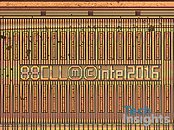
Intel's 10 nanometer FinFET silicon fabrication is coming together at a slower than expected rate, however when it does, it could vastly enlarge the canvas for the company's chip designers, according to a technical report by Tech Insights. The researchers removed the die of an Intel "Cannon Lake" Core i3-8121U processor inside a Lenovo Ideapad330, and put it under their electron microscope.

Its summary mentions quite a few juicy details of the 10 nm process. The biggest of these is the achievement of a 2.7-times increase in transistor density over the current 14 nm node, enabling Intel to cram up to 100.8 million transistors per square millimeter. A 127 mm² die with nothing but a sea of transistors, could have 12.8 billion transistors. Intel 10 nm node also utilizes third-generation FinFET technology, with a reduction in minimum gate pitch from 70 nm to 54 nm; and minimum metal pitch from 52 nm to 36 nm. 10 nm also sees Intel introduce metallization of cobalt in the bulk and anchor layers of the silicon substrate. Cobalt emerged as a good alternative to tungsten and copper as a contact material between layers, due to its lower resistance at smaller sizes,

IBM Research Alliance Builds New Transistor for 5 nm Technology

IBM, its Research Alliance partners GLOBALFOUNDRIES and Samsung, and equipment suppliers have developed an industry-first process to build silicon nanosheet transistors that will enable 5 nanometer (nm) chips. The details of the process will be presented at the 2017 Symposia on VLSI Technology and Circuits conference in Kyoto, Japan. In less than two years since developing a 7 nm test node chip with 20 billion transistors, scientists have paved the way for 30 billion switches on a fingernail-sized chip.

The resulting increase in performance will help accelerate cognitive computing, the Internet of Things (IoT), and other data-intensive applications delivered in the cloud. The power savings could also mean that the batteries in smartphones and other mobile products could last two to three times longer than today's devices, before needing to be charged.

Intel Announces 3rd Generation Core "Ivy Bridge" Processor Family

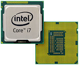
Intel finally got the ball rolling on its third generation Core processor family codenamed "Ivy Bridge", which will go into making most of the company's client processor portfolio for 2012. These chips are characterized as being the world's first microprocessors built on the 22 nanometer silicon fabrication process. Intel aided miniaturization of circuits to such tiny scale thanks to 3D Transistor technology, a space-efficient nano-scale transistor design that enables chip-designers to achieve higher transistor densities, and come up with ever more powerful chips.

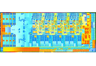
The third-generation Core processor family is based around a single die design (pictured below), from which it will carve out numerous SKUs in the client market in May-June, and enterprise market (under its Xeon brand, towards the end of June). These SKUs will be carved out by toggling the various parallel components (such as x86 cores, cache banks, processor graphics cores, and of course clock-speeds). The new Core processor family is expected to feature higher performance per clock-speed, and higher efficiency. Intel's Kirk Skaugen has been quoted by the BBC as saying "This is the world's first 22 nm product and we'll be delivering about 20% more processor performance using 20% less average power."

Common Platform Transitions to Adopt FinFET 3D Transistor with 14 nm Fab Process

Common Platform, a consortium of three major silicon fabrication companies: IBM, Samsung, and GlobalFoundries, met at their 2012 Technology Forum, where they announced their intention to transition to FinFET 3D transistor technology, but only with the 14 nanometer (nm) silicon fabrication process. Chips on this process will be built in the 2014~2015 time-frame. 3D transistors is a technology pioneered by Intel, which provides space-optimized, energy-efficient transistors on a nano-scale.

FinFET transistors will be combined with Fully Depleted Silicon-On-Insulator (FD-SOI) to offer extremely high transistor densities, with lower chip power. FD-SOI overcomes the limitation of current partially-depleted SOI (PD-SOI) technology, of lower-yields due to the pressure required for SOI insulation, which nears the breaking-point of strained silicon transistors. FinFET tech will be combined with chip-stacking technology, which helps make devices with better use of available PCB footprint.

GK104 Transistor Count and Exact Die-Size Revealed

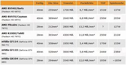
A part of the reason why NVIDIA's performance-segment GK104 is gunning for the performance crown from AMD's Tahiti GPU could be hidden behind two of its key specifications: transistor count, and die-size. 3DCenter.org compiled these two specifications for the GK104 from reliable sources, which pin the transistor count at 3.54 billion, and die-area at 294 mm². This yields a transistor density of 12 million per mm², which is slightly higher than that of AMD Tahiti, slightly lower than that of AMD Pitcairn, and certainly higher than previous-generation chips from both AMD and NVIDIA. If GeForce GTX 680 does in fact end up competitive with AMD's Radeon HD 7900 series, it could serve as a tell-tale sign of NVIDIA's Kepler architecture being a more efficient one.

Scientists Invent First Functional Single-Atom Transistor

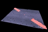
A team of scientists at the ARC Centre for Quantum Computation and Communication, at the University of New South Wales (UNSW), unveiled a fully functional single-atom transistor, which they predict will go on to become a critical building block of tomorrow's high-performance computing devices. The new transistor design was described in a paper, published by Nature. The active component of this transistor is a single phosphorous atom patterned between atomic-scale electrodes and control gates.

Single atom transistor designs have been attempted in the past, but those designs have had an error of about 10 nanometres in positioning of the atoms, which is big enough to affect their functionality. Professor Michelle Simmons, group leader of this study, said that this is the first time "anyone has shown control of a single atom in a substrate with this level of precise accuracy," adding that "Several groups have tried this, but if you want to make a practical computer in the long-term you need to be able to put lots of individual atoms in."

A video presentation by the group follows.

IBM Creates 9 nm Transistors Using Carbon Nanotubules

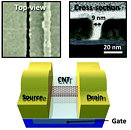
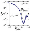
Researchers at IBM have developed the smallest carbon nanotubule transistor, that is 9 nanometers (nm) across. In comparison, the smallest transistors possible using silicon is 10 nm across. IBM claims its new transistor consumes less power while being able to carry more current than today's technology.

"The results really highlight the value of nanotubes in the most sophisticated type of transistors," says John Rogers, professor of materials science at the University of Illinois at Urbana-Champaign. "They suggest, very clearly, that nanotubes have the potential for doing something truly competitive with, or complementary to, silicon." Currently, the smallest production-grade transistors are 22 nm across.
Return to Keyword Browsing
Apr 25th, 2024 17:27 EDT change timezone

New Forum Posts

Popular Reviews

Controversial News Posts