News Posts matching #14 nm

Return to Keyword Browsing

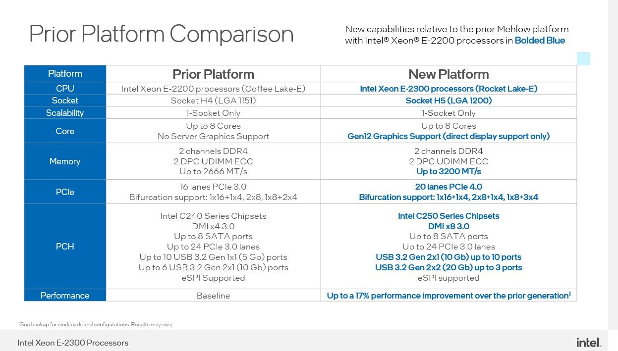
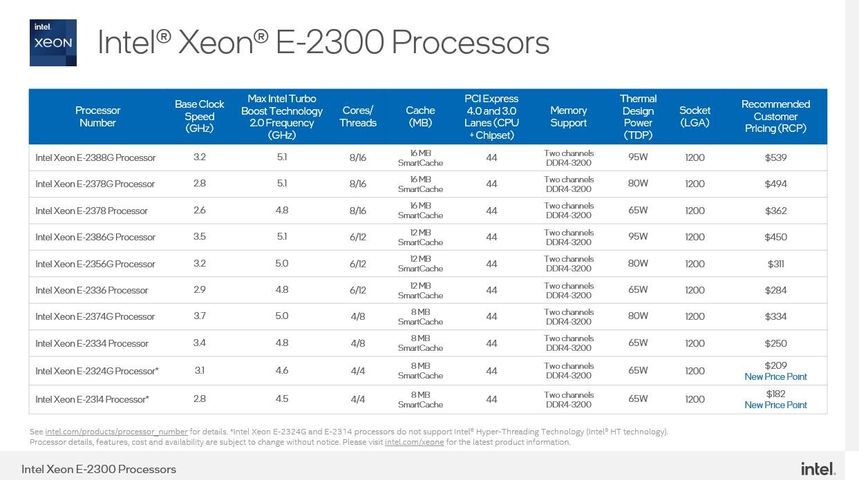
Chinese Company Revives AMD Vega GPU in a Unique NAS Motherboard

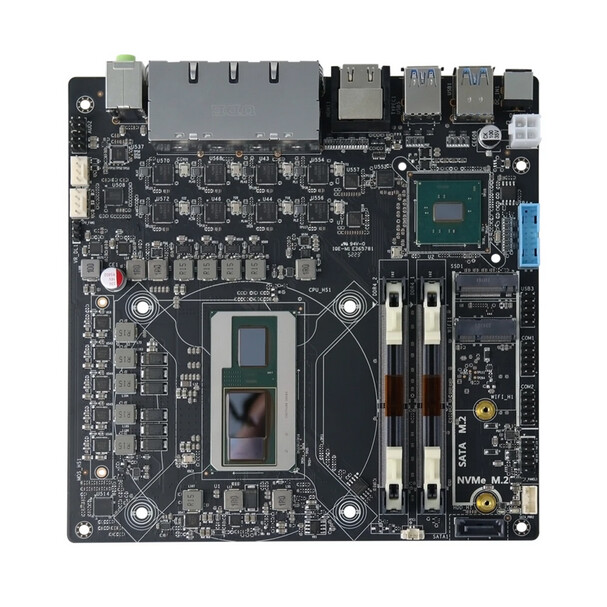
A Chinese Topton company has brought new life to the AMD Vega graphics architecture by integrating it into a Network Attached Storage (NAS) motherboard. The Topton N9 NAS motherboard features the Intel Core i7-8705G processor, a unique chip that combines Intel CPU cores with AMD's RX Vega M GL graphics. The Intel Core i7-8705G, initially released in 2018, is an unusual choice for a NAS system. This 14 nm processor features four cores, eight threads, and a boost clock of up to 4.1 GHz. What sets it apart is the integrated AMD RX Vega M GL GPU with 20 Compute Units and 4 GB of HBM2 memory.

The Topton N9 NAS motherboard is designed for the 17×17 cm ITX form factor and offers a range of features like maximum support for 64 GB of DDR4 RAM, M.2 NVMe/SATA and SATA 3.0, eight Intel i226-V controllers for 2.5 Gbit networking, USB 3.0, USB Type-C, and HDMI 2.0 connectivity. While the Intel Core i7-8705G may not be the most obvious choice for a NAS system, the Topton N9 motherboard demonstrates how this unique processor can be repurposed to provide affordable computing power. The integrated AMD RX Vega graphics offer capabilities beyond typical NAS requirements, making this motherboard suitable for various applications, such as home firewalls and routers. The collaboration between Intel and AMD in creating the Kaby Lake-G processors was a rare occurrence in the industry. The Topton N9 starts at $288.56 without a fan/cooler, and adding another $20 bumps the price to $308.46.

DEEPX Announces State-of-the-Art AI Chip Product Lineup

DEEPX, a leading AI semiconductor technology company, aims to drive innovation in the rapidly evolving edge AI landscape with its state-of-the-art, low-power, high-performance AI chip product lineup. With a focus on revolutionizing application areas such as smart cities, surveillance, smart factories, and other industries, DEEPX unveiled its latest AI semiconductor solutions at the 2023 Samsung Foundry Forum (SFF), under the theme of "For AI Everywhere."

Recognizing the importance of collaboration and technological partnerships, DEEPX leveraged Samsung Electronics' foundry processes, harnessing the power of 5 nm, 14 nm, and 28 nm technologies for its semiconductor chip designs. As a result, the company has developed a suite of four high-performance, energy-efficient AI semiconductor products: DX-L1, DX-L2, DX-M1, and DX-H1. Each product has been specifically engineered to cater to the unique demands of various market segments, from ultra-compact sensors with minimal data processing requirements to AI-intensive applications such as robotics, computer vision, autonomous vehicles, and many others.

Intel Gemini Lake Refresh Reaches End of Life

Intel has posted two product change notifications regarding the Gemini Lake Refresh, which is now reaching the end of its life. Launched in 2019 as a refresh to the original Gemini Lake, these low-end products had a longer lifespan than the original Gemini Lake (2017-2020). Most commonly found on low-end PCs, AIOs, and Mini PCs, these Gemini Lake Refresh CPUs were based on the 14 nm Goldmont Plus microarchitecture. Coming with up to four cores without HyperThreading, these CPUs were ideal for lower-power applications as their TDP was rated between 6-10 Watts.

Intel has separated the product change into two categories, with the first consisting of Celeron N4120, Celeron 4020, and Pentium Silver N5030, while the other features Celeron J4025, Pentium Silver J5040, Celeron N4020C, and Celeron J4125. Intel will ship the first group of CPUs by May 24, 2024, and the second by February 23, 2024. The last round of orders will go out by November 24, 2023, and August 25, 2023, respectively.

Strict Restrictions Imposed by US CHIPS Act Will Lower Willingness of Multinational Suppliers to Invest

TrendForce reports that the US Department of Commerce recently released details regarding its CHIPS and Science Act, which stipulates that beneficiaries of the act will be restricted in their investment activities—for more advanced and mature processes—in China, North Korea, Iran, and Russia for the next ten years. The scope of restrictions in this updated legislation will be far more extensive than the previous export ban, further reducing the willingness of multinational semiconductor companies to invest in China for the next decade.

CHIPS Act will mainly impact TSMC; and as the decoupling of the supply chain continues, VIS and PSMC capture orders rerouted from Chinese foundries
In recent years, the US has banned semiconductor exports and passed the CHIPS Act, all to ensure supply chains decoupling from China. Initially, bans on exports were primarily focused on non-planar transistor architecture (16/14 nm and more advanced processes). However, Japan and the Netherlands have also announced that they intend to join the sanctions, which means key DUV immersion systems, used for producing both sub-16 nm and 40/28 nm mature processes, are likely to be included within the scope of the ban as well. These developments, in conjunction with the CHIPS Act, mean that the expansion of both Chinese foundries and multinational foundries in China will be suppressed to varying degrees—regardless of whether they are advanced or mature processes.

Huawei Reportedly Develops Chip Design Tools for 14 nm and Above

Amid the US sanctions, Chinese technology giant Huawei has reportedly developed tools to create processors with 14 nm and above lithography. According to Chinese media Yicai, Huawei and its semiconductor partners have teamed up to create replacement tools in place of US chip toolmakers like Cadence, Synopsys, and Mentor/Siemens. These three companies control all of the world's Electronic Design Automation (EDA) tools used for every step of chip design, from architecture to placement and routing to the final physical layout. Many steps need to be taken before making a tapeout of a physical chip, and Huawei's newly developed EDA tools will help the Chinese industry with US sanctions which crippled Huawei for a long time.

Having no access to US-made chipmaking tools, Huawei has invested substantial time into making these EDA tools. However, with competing EDA makers supporting lithography way below 14 nm, Huawei's job still needs to be completed. Chinese semiconductor factories are currently capable of 7 nm chip production, and Huawei itself is working on making a sub-7 nm EUV scanner to aid manufacturing goals and compete with the latest from TSMC and other. If Huawei can create EUV scanners that can achieve transistor sizes smaller than 7 nm, we expect to see their EDA tools keep pace as well. It is only a matter of time before they announce adaptation for smaller nodes.

AMD Explains the Economics Behind Chiplets for GPUs

AMD, in its technical presentation for the new Radeon RX 7900 series "Navi 31" GPU, gave us an elaborate explanation on why it had to take the chiplets route for high-end GPUs, devices that are far more complex than CPUs. The company also enlightened us on what sets chiplet-based packages apart from classic multi-chip modules (MCMs). An MCM is a package that consists of multiple independent devices sharing a fiberglass substrate.

An example of an MCM would be a mobile Intel Core processor, in which the CPU die and the PCH die share a substrate. Here, the CPU and the PCH are independent pieces of silicon that can otherwise exist on their own packages (as they do on the desktop platform), but have been paired together on a single substrate to minimize PCB footprint, which is precious on a mobile platform. A chiplet-based device is one where a substrate is made up of multiple dies that cannot otherwise independently exist on their own packages without an impact on inter-die bandwidth or latency. They are essentially what should have been components on a monolithic die, but disintegrated into separate dies built on different semiconductor foundry nodes, with a purely cost-driven motive.

Eliyan Closes $40M Series A Funding Round and Unveils Industry's Highest Performance Chiplet Interconnect Technologies

Eliyan Corporation, credited for the invention of the semiconductor industry's highest-performance and most efficient chiplet interconnect, today announced two major milestones in the commercialization of its technology for multi-die chiplet integration: the close of its Series A $40M funding round, and the successful tapeout of its technology on an industry standard 5-nanometer (nm) process.

Eliyan's NuLink PHY and NuGear technologies address the critical need for a commercially viable approach to enabling high performance and cost-effectiveness in the connection of homogeneous and heterogenous architectures on a standard, organic chip substrate. It has proven to achieve similar bandwidth, power efficiency, and latency as die-to-die implementations using advanced packaging technologies, but without the other drawbacks of specialized approaches.

US Strengthens China Export Bans, Limiting Access to Manufacturing Technology

The US Department of Commerce is in the process of increasing the stranglehold in tech exports directed to Chinese shores. The move is being made through the delivery of letters to US-based technology companies - namely KLA Corp, Lam Research Corp and Applied Materials Inc. - ordering them to stop the export of machines and equipment that can be used for sub-14 nm manufacturing. The move by the Department of Commerce only has validity for the companies that have been served by such a letter - at least until the Department codifies its newest regulations.

This means that only sellers with approved export licenses can keep doing business with Beijing, thus limiting the US companies China can work with as it aims to achieve at least a degree of self-sufficiency in the latest chipmaking tech. Perhaps the decision has come too late, however, as China's mainstay silicon manufacturing, SMIC, already manufactures chips at the 14 nm process (chips that have been deployed in China's Tinahu Light supercomputer already) and has even showcased manufacturing capability in the 7 nm field. It pays to remember that the US already had applied similar restrictions on equipment experts to China for the better part of two years - which apparently did little to stem China's capability to create increasingly denser semiconductor designs.

AMD Confirms Optical-Shrink of Zen 4 to the 4nm Node in its Latest Roadmap

AMD in its Ryzen 7000 series launch event shared its near-future CPU architecture roadmap, in which it confirmed that the "Zen 4" microarchitecture, currently on the 5 nm foundry node, will see an optical-shrink to the 4 nm process in the near future. This doesn't necessarily indicate a new-generation CCD (CPU complex die) on 4 nm, it could even be a monolithic mobile SoC on 4 nm, or perhaps even "Zen 4c" (high core-count, low clock-speed, for cloud-compute); but it doesn't rule out the possibility of a 4 nm CCD that the company can use across both its enterprise and client processors.

The last time AMD hyphenated two foundry nodes for a single generation of the "Zen" architecture, was with the original (first-generation) "Zen," which debuted on the 14 nm node, but was optically shrunk and refined on the 12 nm node, with the company designating the evolution as "Zen+." The Ryzen 7000-series desktop processors, as well as the upcoming EPYC "Genoa" server processors, will ship with 5 nm CCDs, with AMD ticking it off in its roadmap. Chronologically placed next to it are "Zen 4" with 3D Vertical Cache (3DV Cache), and the "Zen 4c." The company is planning "Zen 4" with 3DV Cache both for its server- and desktop segments. Further down the roadmap, as we approach 2024, we see the company debut the future "Zen 5" architecture on the same 4 nm node, evolving into 3 nm on certain variants.

AMD and GlobalFoundries Renew Wafer Supply Agreement

AMD in its 8-K filing with the SEC, disclosed that it has updated its wafer supply agreement (WSA) with GlobalFoundries. Under the latest agreement, AMD commits to buy $2.1 billion worth wafers from GlobalFoundries between 2022 and 2025. The previous version of the WSA saw commitments up to 2024, and wafers worth $1.6 billion. The update hence adds another year and $500 million worth supply.

AMD currently sources 12 nm and 14 nm wafers from GlobalFoundries, which go into making cIOD and sIOD components in its processors, and motherboard chipsets. The move to extend the WSA indicates that the company may continue to use 12 nm-class I/O dies in its processors for the foreseeable future. It will be very interesting to see if 12 nm-class I/O dies make it to next-generation products such as "Genoa" and "Rapael," which integrate the latest IP blocks such as PCI-Express Gen 5 root-complexes, DDR5 memory controllers, and 3rd Gen Infinity Fabric. Processors with 12 nm I/O dies, such as "Milan" and "Vermeer" could be retired only by 2023-24, as AMD will use 2022 to spread across its next-gen product launches.

Report: DDR5 Already Facing Production Issues In Wake of Global Chip Shortages

DDR5 may soon have reason to be an even more expensive early-adopter piece of tech than it currently is, according to electronic component supplier 12chip. While semiconductor manufacturers worldwide grapple with logistics and components shortages, the DRAM market has been left somewhat unscathed - up to now. DRAM fabrication - even DDR5 - isn't done on leading-edge nodes but on older, more mature ones (such as 14 nm). According to 12chip, manufacturers are having no problem in scaling their DRAM manufacturing on these older nodes to meet demand.

However, DDR5 is being directly impacted by the current logistics issues due to lack of adequate Power Management Integrated Circuit (PMIC) chips - which DDR5 has integrated in the DIMM proper. Currently, lead times for PMIC orders are estimated at 35 weeks, placing additional strain on system assemblers and DRAM manufacturers - and forcing delays and bottlenecks throughout the supply chain. Additionally, the fact that PMIC chips for DDR5 are ten times as expensive as equivalent DDR4 power management solutions doesn't bode well for future price action on DDR. Should this situation continue, higher prices for DDR5 modules are to be expected due to a deteriorating supply/demand ratio - particularly relevant if you're thinking about putting together a build based on Intel's Alder Lake platform. As always, take this report with a grain of salt.

Samsung Develops Industry's First LPDDR5X DRAM

Samsung Electronics Co., Ltd., the world leader in advanced memory technology, today announced that it has developed the industry's first 14-nanometer (nm) based 16-gigabit (Gb) Low Power Double Data Rate 5X (LPDDR5X) DRAM, designed to drive further growth throughout the high-speed data service applications including 5G, artificial intelligence (AI) and the metaverse.

"In recent years, hyperconnected market segments such as AI, augmented reality (AR) and the metaverse, which rely on extremely fast large-scale data processing, have been rapidly expanding," said SangJoon Hwang, senior vice president and head of the DRAM Design Team at Samsung Electronics. "Our LPDDR5X will broaden the use of high-performance, low-power memory beyond smartphones and bring new capabilities to AI-based edge applications like servers and even automobiles."

Samsung Starts Mass Production of Most Advanced 14 nm EUV DDR5 DRAM

Samsung Electronics, the world leader in advanced memory technology, today announced that it has begun mass producing the industry's smallest, 14-nanometer (nm), DRAM based on extreme ultraviolet (EUV) technology. Following the company's shipment of the industry-first EUV DRAM in March of last year, Samsung has increased the number of EUV layers to five to deliver today's finest, most advanced DRAM process for its DDR5 solutions.

"We have led the DRAM market for nearly three decades by pioneering key patterning technology innovations," said Jooyoung Lee, Senior Vice President and Head of DRAM Product & Technology at Samsung Electronics. "Today, Samsung is setting another technology milestone with multi-layer EUV that has enabled extreme miniaturization at 14 nm—a feat not possible with the conventional argon fluoride (ArF) process. Building on this advancement, we will continue to provide the most differentiated memory solutions by fully addressing the need for greater performance and capacity in the data-driven world of 5G, AI and the metaverse."

Samsung Foundry Announces GAA Ready, 3nm in 2022, 2nm in 2025, Other Speciality Nodes

Samsung Electronics, a world leader in advanced semiconductor technology, today unveiled plans for continuous process technology migration to 3- and 2-nanometer (nm) based on the company's Gate-All-Around (GAA) transistor structure at its 5th annual Samsung Foundry Forum (SFF) 2021. With a theme of "Adding One More Dimension," the multi-day virtual event is expected to draw over 2,000 global customers and partners. At this year's event, Samsung will share its vision to bolster its leadership in the rapidly evolving foundry market by taking each respective part of foundry business to the next level: process technology, manufacturing operations, and foundry services.

"We will increase our overall production capacity and lead the most advanced technologies while taking silicon scaling a step further and continuing technological innovation by application," said Dr. Siyoung Choi, President and Head of Foundry Business at Samsung Electronics. "Amid further digitalization prompted by the COVID-19 pandemic, our customers and partners will discover the limitless potential of silicon implementation for delivering the right technology at the right time."

Intel Intros Xeon E-2300 Series Based on 14 nm "Rocket Lake-E"

Intel today released the Xeon E-2300 series enterprise processors for entry level servers, based on the 14 nm "Rocket Lake-E" silicon. These are slightly different from the Xeon W-1300 series processors targeting workstations. The E-2300 has a more server-relevant feature-set, and is designed for high uptime. You get ECC memory support, as well as vPro, SGX, and MPX (memory encryption). You still get only client-relevant AVX-512 instructions found in 11th Gen Core processors, as well as DLBoost AI acceleration.

The "Rocket Lake-E" silicon comes with up to 8 "Cypress Cove" CPU cores, each with 512 KB of dedicated L2 cache, and 16 MB of shared L3 cache. The processor features a 2-channel DDR4 memory interface that supports up to 128 GB of DDR4-3200 memory. It puts out 20 PCI-Express 4.0 lanes that can be segmented in a number of ways; as well as the Intel C250 series chipset puts out 24 PCI-Express 3.0 lanes. Chips in this series come with TDP of up to 95 W.

Foundry Revenue for 2Q21 Reaches Historical High Once Again with 6% QoQ Growth Thanks to Increased ASP and Persistent Demand, Says TrendForce

The panic buying of chips persisted in 2Q21 owing to factors such as post-pandemic demand, industry-wide shift to 5G telecom technology, geopolitical tensions, and chronic chip shortages, according to TrendForce's latest investigations. Chip demand from ODMs/OEMs remained high, as they were unable to meet shipment targets for various end-products due to the shortage of foundry capacities. In addition, wafers inputted in 1Q21 underwent a price hike and were subsequently outputted in 2Q21. Foundry revenue for the quarter reached US$24.407 billion, representing a 6.2% QoQ increase and yet another record high for the eighth consecutive quarter since 3Q19.

Intel "Alder Lake" Silicon Variants Detailed—Reunification of the Product Lines

The 12th Gen Core "Alder Lake" microarchitecture will see Intel unify its desktop- and mobile processor IP, back to the way things were up to the 9th Gen. With its post-14 nm silicon fabrication nodes in their infancy, Intel had diverged the client processor IP across its 10th and 11th Gen Core. With 10th Gen, the company introduced "Ice Lake" for ultra-portable platforms (28 W and below), while retaining 14 nm "Comet Lake" for mainstream notebooks (28 W to 45 W); while keeping desktop exclusively with 14 nm "Comet Lake." For 11th Gen, the story is mostly similar. Cutting-edge 10 nm "Tiger Lake" now covers all mobile categories, while desktop receives an IPC upgrade, thanks to the 14 nm "Rocket Lake." The 12th Gen will see a common microarchitecture, "Alder Lake," span across all client segments, from 7 W ultra mobile, to 125 W enthusiast desktop.

This, however, doesn't mean that Intel has a one-size fits all silicon that it can carve SKUs out of. The company has developed as many as three physical dies based on "Alder Lake," which vary in CPU core counts, the size of the iGPU, and other on-die components. "Alder Lake" is a hybrid processor with a combination of larger "Golden Cove" P-cores, and smaller "Gracemont" E-cores. The P-cores are spatially large, and along with their L3 cache slices, take up a large share of the compute portion of the silicon. The E-cores come in clusters of 4 cores each.

Penetration Rate of Ice Lake CPUs in Server Market Expected to Surpass 30% by Year's End as x86 Architecture Remains Dominant, Says TrendForce

While the server industry transitions to the latest generation of processors based on the x86 platform, the Intel Ice Lake and AMD Milan CPUs entered mass production earlier this year and were shipped to certain customers, such as North American CSPs and telecommunication companies, at a low volume in 1Q21, according to TrendForce's latest investigations. These processors are expected to begin seeing widespread adoption in the server market in 3Q21. TrendForce believes that Ice Lake represents a step-up in computing performance from the previous generation due to its higher scalability and support for more memory channels. On the other hand, the new normal that emerged in the post-pandemic era is expected to drive clients in the server sector to partially migrate to the Ice Lake platform, whose share in the server market is expected to surpass 30% in 4Q21.

Samsung to Build a 5nm EUV Semiconductor Fab in Austin TX

Samsung Electronics plans to build a new cutting-edge semiconductor fab in Austin, Texas, according to an ETimes report. An official announcement to this effect will be made later today, when South Korean President Moon and U.S. President Biden are scheduled to hold their first Summit meeting, in Washington DC. The facility will offer third-party contract manufacturing of semiconductor chips on the 5 nanometer EUV process. Samsung has earmarked an investment of $18 billion toward the construction of this fab, which will be located close to the company's existing foundry in Texas, which manufactures chips on the 14 nm node. Samsung's investment is in response to rising demand of high-volume logic chips by major American firms such as Amazon, Google, Microsoft, and Tesla.

Intel Core-1800 Alder Lake Engineering Sample Spotted with 16C/24T Configuration

Intel's upcoming Alder Lake generation of processors is going to be the first iteration of heterogeneous x86 architecture. That means that Intel will for the first time combine smaller, low-power cores, with some big high-performance cores to provide the boost to all the workloads. If a task doesn't need much power, as some background task, for example, the smaller cores are used. And if you need to render something or you want to fire up a game, big cores are used to provide the power needed for the tasks. Intel has decided to provide such an architecture on the advanced 10 nm SuperFin, which represents a major upgrade over the existing 14 nm process.

Today, we got some information from Igor's Lab, showing the leaked specification of the Intel Core-1800 processor engineering sample. While this may not represent the final name, we see that the leaked information shows that the processor is B0 stepping. That means that the CPU will see more changes when the final sample arrives. The CPU has 16 cores with 24 threads. Eight of those cores are big ones with hyperthreading, while the remaining 8 are smaller Atom cores. They are running at the base clock of 1800 MHz, while the boost speeds are 4.6 GHz with two cores, 4.4 GHz with four cores, and 4.2 GHz with 6 cores. When all cores are used, the boost speed is locked at 4.0 GHz. The CPU has a PL1 TDP of 125 Watts, while the PL2 configuration boosts the TDP to 228 Watts. The CPU was reportedly running at 1.3147 Volts during the test. You can check out the complete datasheet below.

Foundry Revenue Projected to Reach Historical High of US$94.6 Billion in 2021 Thanks to High 5G/HPC/End-Device Demand, Says TrendForce

As the global economy enters the post-pandemic era, technologies including 5G, WiFi6/6E, and HPC (high-performance computing) have been advancing rapidly, in turn bringing about a fundamental, structural change in the semiconductor industry as well, according to TrendForce's latest investigations. While the demand for certain devices such as notebook computers and TVs underwent a sharp uptick due to the onset of the stay-at-home economy, this demand will return to pre-pandemic levels once the pandemic has been brought under control as a result of the global vaccination drive. Nevertheless, the worldwide shift to next-gen telecommunication standards has brought about a replacement demand for telecom and networking devices, and this demand will continue to propel the semiconductor industry, resulting in high capacity utilization rates across the major foundries. As certain foundries continue to expand their production capacities this year, TrendForce expects total foundry revenue to reach a historical high of US$94.6 billion this year, an 11% growth YoY.

Intel Readies Xeon W-1300 Socket LGA1200 Processors Based on "Rocket Lake"

Intel is reportedly giving final touches to the Xeon W-1300 line of enterprise processors targeting workstations, according to an ASRock CPU support list dug up by Komachi Ensaka. The processors are based on the same 14 nm "Rocket Lake" silicon as the company's 11th Gen Core desktop processors, and come in core counts of up to 8-core/16-thread. The lineup is expected to debut with five SKUs, three of which are 8-core/16-thread, and two 6-core/12-thread.

The lineup is led by the W-1370, with base frequency of 2.90 GHz, 16 MB of shared L3 cache, and 80 W TDP. Next up, is the slightly slower W-1390, clocked at 2.80 GHz, and 80 W TDP. The third 8-core part is the W-1390T, which is clocked at just 1.50 GHz (base), and comes with aggressive power-management that gives it a TDP rating of 35 W. The 6-core/12-thread W-1350P has the highest clock speeds, with a base frequency of 4.00 GHz, 12 MB of shared L3 cache, and 125 W TDP. The W-1350 is its slower sibling, clocked at 3.30 GHz, and 80 W TDP. The processors will be compatible with Intel Z490, W480, and H470 chipsets, besides their 500-series successors.

Intel to Unveil "Tiger Lake-H" and "Rocket Lake-S" on March 18

Intel is expected to unveil its 11th generation Core "Tiger Lake-H" performance-segment mobile processor, and the highly anticipated 11th Gen Core "Rocket Lake-S" desktop processor family on March 18, 2021. The two will be launched on the sidelines of the 2021 GDC (Game Developers Conference), an online event. The agenda page of GDC mentions both "Tiger Lake-H" and "Rocket Lake." The "Tiger Lake-H" family of processors begin with quad-core SKUs based on the 4-core "Tiger Lake" silicon, extending to 6-core and 8-core ones based on a newer 8-core silicon. Both dies are built on the 10 nm SuperFin node, and combine Intel's highest-IPC "Willow Cove" CPU cores with a Gen 12 Xe iGPU.

The 11th Gen Core "Rocket Lake-S" has been unveiled back at the 2021 International CES (online event) in January, and is heading toward a mid/late-March launch. The chips pack up to eight "Cypress Cove" CPU cores, which are a back-port of Intel's 10 nm CPU core architectures to the 14 nm node, bringing the first IPC increase on the client desktop platform from Intel since 2015. At GDC, we expect Intel to detail individual SKUs within the 11th Gen Core processor family, giving us a broader idea of what chips will launch this month. The GDC backdrop also foreshadows the marketing strategy for Intel with both these platforms—gaming. The company will take advantage of the IPC uplift to present its processors as being better for gaming, and sufficiently fast in most client-relevant tasks. The GDC backdrop could also let Intel show off the ISV relations it's built with game developers, detailing how certain popular game engines are optimized for Intel.

Intel Core i9 and Core i7 "Rocket Lake" Lineup Leaked, Claims Beating Ryzen 9 5900X

Intel is planning to debut its 11th Generation Core "Rocket Lake-S" desktop processor family with a fairly large selection of SKUs, according to leaked company slides shared by VideoCardz, which appear to be coming from the same source as an earlier report from today that talk about double-digit percent gaming performance gains over the previous generation. Just the Core i9 and Core i7 series add up to 10 SKUs between them. These include unlocked- and iGPU-enabled "K" SKUs, unlocked but iGPU-disabled "KF," locked but iGPU-enabled parts, and locked and iGPU-disabled "F" parts.

With "Rocket Lake-S," Intel appears to have hit a ceiling with the number of CPU cores it can cram onto a die alongside an iGPU, on the 75 mm x 75 mm LGA package, while retaining its 14 nm silicon fabrication node. Both the Core i9-11900 series and the Core i7-10700 series are 8-core/16-thread parts, with an identical amount of cache. They are differentiated on the basis of clock speeds as tabled below, and the lack of the Thermal Velocity Boost feature on the Core i7 parts. The Core i5 series "Rocket Lake-S" parts are reportedly 6-core/12-thread.

Intel Core i9-11900K "Rocket Lake" Gaming Performance Leaked

An alleged Intel marketing slide highlighting the gaming performance advances of the company's upcoming Core i9-11900K "Rocket Lake" processor was leaked to the web. The slide compares the i9-11900K to the previous generation i9-10900K "Comet Lake-S," showing that despite two fewer CPU cores, the new chip is able to post double-digit percent gaming performance gains. At 1080p resolution, which is relevant to CPU testing as it highlights bottlenecks at the CPU-level, the i9-11900K is claimed to gain over 13% in frame-rates with "Total War: Three Kingdoms," and a significant 14% with Microsoft Flight Simulator. "Gears 5" shows a 9% performance gain, while GRID 2019 is 8% faster.

The Core i9-11900K owes its gaming performance gains to the IPC increase (single-thread performance increase) from the new "Cypress Cove" CPU cores. The "Rocket Lake-S" silicon features up to 8 "Cypress Cove" cores, which are believed to be a back-port of the "Willow Cove" core to the 14 nm silicon fabrication node, albeit with modifications, such as lower L2 cache sizes. Intel is looking to restore PC gaming performance leadership with the 11th Gen Core desktop processor series. The chips are expected to launch later this month.
Return to Keyword Browsing
Apr 19th, 2024 15:34 EDT change timezone

New Forum Posts

Popular Reviews

Controversial News Posts