News Posts matching #G200b

Return to Keyword Browsing

EVGA and NVIDIA Design Unique Multi-GPU Graphics Accelerator

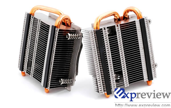
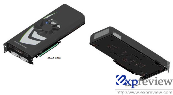
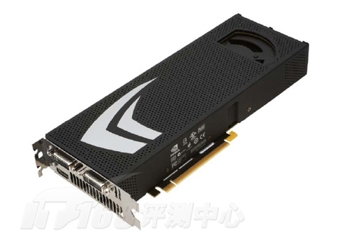
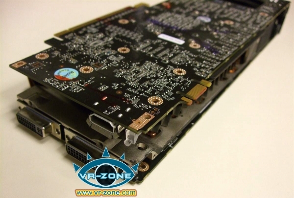
EVGA and NVIDIA are readying a unique multi-GPU graphics accelerator this Halloween, slated for October 30. To celebrate its launch, the two have organized a launch party for 300 lucky participants who will go to the NVIDIA Plaza in Santa Clara, CA and witness the launch of the new GeForce product. The accelerator packs two GPUs: a G200b, and a G92b. That's right, a GeForce GTX 200 series GPU, with a GeForce GTS 250 GPU. This is perhaps the first graphics accelerator to pack two entirely different GPUs. How it works, however, is interesting: the G200b GPU handles graphics, while the G92b is dedicated to PhysX processing. The accelerator could have 896 MB of graphics memory, with 512 MB of dedicated memory for the PhysX GPU. You can sign up for the event here.

EVGA Rolls out 4-way SLI Compatible GeForce GTX 285 Accelerator

ASUS stirred up the enthusiast community recently with its dual-GeForce GTX 285 accelerator that for the first time, lets four fully-loaded G200b GPUs function in quad-SLI. Perhaps responding to it, EVGA rolled out the EVGA GeForce GTX 285 Classified (01G-P3-1190-AR), the first single-GPU GeForce accelerator to support 4-way SLI (or Quad-SLI). With a small but significant number of SLI-compatible motherboards with four PCI-Express x16 slots already out there, EVGA hopes to cash in with its newest product.

The GeForce GTX 285 Classified sticks to reference NVIDIA clock speeds of 648/1242 MHz (core/memory), while leaving it to the user to overclock it, by providing a number of design enhancements. It also sticks to having 1 GB of memory. To begin with, this card features a full 8-phase digital-PWM power design, and makes use of high-grade components such as film capacitors. It draws power from three 6-pin PCI-E power connectors. Voltage measure points for VPLL, DRAM VDDQ, DRAM VDD, and VGPU are nucleated in a convenient location for easy measurements. The card supports EVGA's EVbot device that provides control over the card's parameters in the hands of the user. The EVbot can be directly plugged in to the card. Finally, the card supports 4-way SLI. At this point what its SLI bridge looks like is not known, but hopefully it's provided with the card or the EVGA's newest motherboard. It has been listed on the company store for US $379.99, currently on pre-order.

First Single-PCB GeForce GTX 295 Accelerator Spotted

So it is true! NVIDIA does have a single-PCB GeForce GTX 295 accelerator in the works, and partners already seem to have access to it. The card must have had some serious development put into it, given the sheer complexity of the PCB (to cram two G200b GPUs, their display processors, and the PCI-E bridge chip, along with 28 memory chips). The accelerator first surfaced in the form of CAD drawings, in March.

The PCB is pretty straight-forward: populate all the important logic on its business-side, and the memory on either sides. The card maintains its requirement for 8 + 6 pin PCI-E power input. Its VRM is spread across two main areas, to power a GPU system each. Internal SLI connects the two systems, while also providing support for Quad-SLI. Each GPU features 240 shader processors, along with 896 MB of GDDR3 memory across a 448-bit memory interface. Also pictured is the cooler: A fan nucleates the cooler, and blows in two opposite directions. The air is guided by the shroud onto two dense aluminum fin arrays that cool each GPU-system. The back of the card may use a heatspreader to cool the memory, like how the GeForce GTX 280 does it. While we don't expect this design to bring down the retail price of the card, we do believe that the design is mainly to provide partners, and retailers with decent margins that make selling the card a worthwhile venture. With the older design, it might not have been the case.

NVIDIA Outsources 40 nm to Foundry Partners in Q2

With rival AMD having a production-grade 40 nm graphics processor, and UMC's recent announcement of being ready with a high-performance 40 nm manufacturing node, the conditions are increasingly favourable for NVIDIA to flag-off large-scale production of 40 nm GPUs. According to Chinese print-media Commercial Times, the company set its foundry outsourcing schedule for within Q2 2009, with TSMC and UMC being the regular foundry-partners.

Within this quarter, NVIDIA will start mass-production of the entry-level GT218, high-end mobile GT215 and mainstream desktop GT214 and GT216 GPUs. Additionally, the company may also expand its output for the 55 nm G200b high-end GPU.

GeForce GTX 275 Catches Early Flight, Launch Brought Forward to April 2

As reviewers world-over unbox their Radeon HD 4890 samples, NVIDIA, in a last-bid attempt not to give ATI a fortnight's headstart over GeForce GTX 275, has pulled its launch forward to April 2, the day Radeon HD 4890 hits shelves. Our sources however, indicate that this will be merely a paper-launch for NVIDIA, meaning that the actual product doesn't exist in retail channels, only that its SKU officially exists, get listed, perhaps gets open to pre-orders by retailers, and what's more, even previewed.

It will be mid-April by the time retailers actually start to sell GeForce GTX 275 accelerators. The accelerators will be of non-reference designs, with the specifications we know so far: 55 nm G200b GPU, 240 stream processors, 448-bit GDDR3 memory interface, and 896 or 1792 MB of memory. The clock speeds the card will run at are known to be 633/1404/1138 MHz (core/shader/memory). Its price will be very competitive with that of the Radeon HD 4890, around the US $250 mark.

Single-PCB GeForce GTX 295 in the Works

Traditionally, NVIDIA designs dual-GPU accelerators with two PCBs holding a GPU system each. With the GeForce GTX 295 and its competitive pricing, NVIDIA found itself in a difficult position, as it faces direct competition from ATI with its now competitively priced Radeon HD 4870 X2. On the one hand, escalating manufacturing costs due to extreme competition with the sub-$300 graphics card market, is making it difficult for NVIDIA to keep up with GTX 295 stocks, on the other its repercussions that include bad press and losses due to not being able to keep up with demand, have pushed NVIDIA to rethink a way to make the GeForce GTX 295.

Enter innovation. The company is reportedly redesigning the GeForce GTX 295, this time on a single PCB design, which ATI has been using for its dual-GPU accelerators. Both GPU systems of the GTX 295 will be placed on a single PCB. This is expected to significantly bring down manufacturing costs, allowing the company to keep up with demands and competitive pricing. Expreview sourced the drawings of one of the prototypes, which shows a long single PCB card, with a central fan. You will also observe that there is a back-plate in place. It shows that a number of memory chips will be populated on the back, and both GPU systems on the front. It will be an engineering challenge, to populate five major heat-producing components (two G200b GPUs, two NVIO2 processors, and one BR-03 bridge chip), 28 GDDR3 memory chips, and the VRM area to power it all. The new redesigned card may surface internally in April, and may enter production by May.

NVIDIA Preparing GeForce GTX 275, RV790XT in Sights

AMD is on the course of releasing a new line of high performance products based on its upcoming RV790 graphics processor. The high-end single GPU SKU, Radeon HD 4890 is expected to be competitive with NVIDIA's GeForce GTX 260 (216 SP). NVIDIA on the other end of the field, is planning a retaliation to the RV790. The GPU giant is carving out a new SKU based on the 55 nm G200b: GeForce GTX 275.

The new SKU will be placed in the US $225~275 range. While the specifications are not known at this point in time, there are two theories: G200b with 216 stream processors and a 512-bit memory interface, and the other theory suggesting 240 stream processors with the existing 448-bit memory interface on GTX 260. The latter looks inexpensive as the former would step up manufacturing costs due to the addition of two memory chips.

Radeon HD 4890 X2 a Reality On The Basis of Performance Against Competitor

AMD is attempting to revive its competitiveness that took a beating with NVIDIA's introduction of 55 nm G200b-based graphics accelerators. The method AMD seems to be adopting is by giving its existing flagship GPU, the RV770, a series of design improvements that facilitate higher clock-speeds, in turn, better performance on offer.

A lot has been said about RV790 till date, with each commentator coming up with a new version of the story. It has been more or less established that the RV790 will be a improvement over the RV770, though not a revolutionary one. Fresh information gathered by PC Games Hardware places a realistic estimate on up to where RV790 is going to push the performance envelope for AMD.

ASUS Preparing GeForce GTX 285 Ultimate

ASUS is reportedly preparing a new variant in its GeForce GTX 285 lineup: the ENGTX285-UL/HTDI/1GD3 "Ultimate". ASUS seems to have done away with using the "TOP" branding to denote the fastest variant in a given graphics card series. ASUS stuck with the NVIDIA reference design for this variant, while looking to squeeze out the most factory overclocking the reference design has to offer.

The ASUS GeForce GTX 285 Ultimate boasts clock speeds of 712/1620/1380 MHz (core/shader/memory). The card finds competition in EVGA's GeForce GTX 285 FTW, which has similar, albeit slightly higher clock speeds. The rest of its specifications remain standard, having the 55 nm G200b core, 240 stream processors, 1 GB of GDDR3 memory across a 512-bit wide memory bus, and support for 3-way SLI. ASUS may look to price it in the US $449 price point.

Galaxy Releases GeForce GTX 260+ Non-Reference Card, Changes Cooling Specifications

Galaxy finally pushed its self-designed GeForce GTX 260+ graphics card to retail. The card surfaced earlier this month, in a pre-release appearance with a completely different GPU cooler (read here). The pre-release iteration featured PC-Cooler HP4-1226. As we found out during the course of the discussion, the said cooler was too large to be sold with the card, as it would probably span across four or more expansion slots.

Galaxy made the release-grade card a bit more retail-friendly by using a slightly modified Accelero Twin-Turbo cooler made by Arctic Cooling. The new cooler keeps the footprint of this card within three expansion slots. The Galaxy GeForce GTX 260+ features factory-overclocked parameters, of 625/1350/1050 MHz (core/shader/memory), a 7% overclock over the reference speeds. It uses the 55 nm G200b core, with 216 stream processors and 896 MB of GDDR3 memory. Interestingly, the card bundles Galaxy's Xtreme Tuner overclocking software, as against the Magic Panel software the pre-release iteration was spotted with, by Chinese media.

Zotac Readying Custom-Design GTX 285 Accelerator

NVIDIA seems to have lifted restrictions over manufacturers coming up with their own designs for the GeForce GTX 285 accelerator, barely a month into its market introduction. Zotac, backed by the engineering prowess of PCPartner seems to have already designed their custom-PCB according to a finding by Expreview. The new PCB employs a decent bit of component rearrangement.

Perhaps the most significant part of that rearrangement comes from moving the vMem circuit that powers the card's 16 memory chips to its anterior end, in between the NVIO2 processor and the SLI connectors. The PCB uses a new MOSFET arrangement that groups them in a DPAK group. The vGPU circuit consists of 6 phases, and the vMem circuit 2. Zotac makes use of an aluminum support-brace around the G200b graphics processor, which serves as a safety measure for the GPU, minimizing the impact of PCB bending on the fragile ball-grid, especially with 55nm GeForce GTX 260 and GTX 285 lacking a back-plate that counters PCB bending. The orange-coloured DVI connectors make it distinctively Zotac. The SKU based on the new PCB may feature reference clock speeds of 648/2484/1476 MHz (core/memory/shader). Its cooler design remains unknown.

NVIDIA Designs New GTX 260 PCB, Further Reduces Manufacturing Costs

The introduction of the new G200b series graphics processors sought to revive NVIDIA's stronghold over the high-end graphics market, by reducing manufacturing costs, and facilitating high-end graphics cards at unusually low price-points, to compete with rival ATI. The first SKU using the G200b GPU was the new GeForce GTX 260. The PCB of design of the new model (P654) saw several drastic changes, that also ended up contributing to the cost-cutting: all memory chips were placed in the business end of the PCB, and the VRM area rearranged. News emerging from Expreview suggests that NVIDIA has worked out an even newer PCB reference design (model: P897) that aims mainly to cut production costs further. The reference design graphics board based on the PCB will be given the internal name "D10U-20". A short list of changes is as follows:
  • The number of PCB layers has been reduced from 10 to 8, perhaps to compress or remove blank, redundant or rudimentary connections
  • A 4+2 phase NVVDD power design using the ADP4100 voltage regulator IC, the FBVDDQ circuit has been reduced from 2 phases to 1, and the MOSFET package has been changed from LFPAK to DPAK grouping, to reduce costs. The ADP4100 lacks the I2C interface, which means voltage control will be much more difficult than on current PCBs of the GeForce 260,280, 285 and 295
  • The optional G200b support-brace has been removed
  • While the length of the PCB remains the same, the height has been reduced to cut costs
  • BIOS EEPROM capacity reduced from 1 Mbit (128 KB) to 512 Kb (64 KB)
  • Cheaper DVI connectors

MSI Starts off With Overclocked GeForce GTX 285

Graphics card manufacturers either release entire lineups of products based on a particular GPU on one go, comprising of a base-model sticking to the GPU vendors' reference specifications, all the way up to factory-overclocked cards, or they release base-models first and follow it up with overclocked variants later. MSI did the opposite, with starting its GeForce GTX 285 lineup with a "base-model" that doesn't adhere to reference clock speeds by NVIDIA, but instead, comes slightly overclocked.

The MSI GeForce GTX 285 (model: N285GTX-T2D1G-OC), the company's first entry to its N285GTX series, comes with clock speeds of 680 MHz (core), 1476 MHz (shader) and 2484 MHz (memory). These, against the NVIDIA reference clock speeds of 680/1476/1998 MHz. The GeForce GTX 285, as we know, is based on the G200b graphics processor. It is built on the 55nm manufacturing node of TSMC. It features 240 stream processors and 1 GB of GDDR3 memory across a 512-bit wide memory bus. The MSI N285GTX-T2D1G-OC should make it by January 15.

GeForce GTX 285 Reviewed, Lives-Up to Company Projections

NVIDIA looks to restore the market position it lost to ATI in the past two quarters. Its plans will be spearheaded by the G200b graphics processor, on which are based products that outperform and offer better value than ATI products in its price-bands. The GeForce GTX 280 lost its position as the fastest graphics card to the Radeon HD 4870 X2. While NVIDIA is looking to establish itself as the maker of the fastest grachics card with the dual-G200b based GeForce GTX 295, the Radeon HD 4800 Series faces a two-pronged attack from NVIDIA's products, in which the GeForce GTX 285, will fit in as a sub-$400 product that looks to be "too good for its price to opt for a Radeon HD 4870 X2". The GeForce GTX 285 comes with reference clock-speeds of 648 MHz (core), 1476 MHz (shader) and 2484 MHz (memory).

German website ComputerBase.de put the GeForce GTX 285 (GeForce GTX 280 overclocked to its specs) through a broad range of games and synthetic benchmarks. Its evaluation found the GeForce GTX 285 living-up to NVIDIA's performance projections when pitted against a GeForce GTX 280, that of increments of roughly 10%. The review was conducted at a set resolution of 1680x1050, with different AA/AF modes.

The full review (in German) can be read here (Google Translated to English).

NVIDIA GPU Lineup for 2009 Tabled

The year 2008 has been eventful for the PC graphics industry. This is the year which, for the most of the part, saw some serious competition between NVIDIA and ATI. While pure horsepower and value are what determined product superiority, implementing new technologies is what looks to drive GPU makers in 2009. One of the first of these technologies is the introduction of the 40nm manufacturing process, which facilitates GPU makers to step-up transistor counts or even cut manufacturing costs. VR-Zone, based on a few documents it has access to, compiled a list of GPUs that NVIDIA could pull out of its hat in 2009.

To begin with, NVIDIA is expected to have a full-fledged lineup of GPUs top-to-bottom built on the 40nm fab process within 2009. Before it makes the move to the new fab process, the G200b, built on the 55nm fab process will be given a chance to hold the performance and enthusiast segment offerings by the company, in Q1. Come Q2, and the G200b will be succeeded by GT212. All that while, current G94, G96, G98 will hold the mainstream thru value segments, only to be replaced by GT214, GT216 and GT218 respectively in Q3. NVIDIA's gets a newer IGP too, the iGT209. NVIDIA looks to end the year with a newer high-end GPU, the GT300 to succeed GT212 in Q4.

RV740 Successfully Taped Out, Other 40nm GPUs Follow

The RV740 graphics processor by AMD could well be the first GPU in production, to be built on the newer 40nm manufacturing process, giving its makers something to brag about. The RV740 design and specifications are largely derived from the RV770LE (covered here), while bringing the GDDR5 memory standard to the mainstream.

Chinese industrial journals tell DigiTimes that the company has completed taping-out the RV740, and that the GPU is awaiting mass-production by AMD's foundry partner, Taiwan Semiconductor Manufacturing Company (TSMC). Mass production of products based on this GPU could commence by the end of Q1 2009.

GeForce GTX 285 Pitted Against GeForce GTX 280

Following the industry-wide launch of the new 55nm GeForce GTX 260, NVIDIA would launch its fastest single-GPU graphics card: the GeForce GTX 285. This card is based on the 55nm G200b core. It has identical specifications to the GeForce GTX 280, except for its higher reference clock speeds, and lower power consumption. Due to these, NVIDIA seems to have given it the "285" number, while the 55nm GTX 260 continues to hold its "260" due to identical reference clock speeds as its 65nm counterparts.

ChipHell sourced two NVIDIA company slides which show some of the specifications of GeForce GTX 285 and its expected level of performance in comparison to the GeForce GTX 280. There is also a little mention about the testing conditions: a Core i7-based machine running 32-bit Windows Vista. Across the various synthetic and real-world gaming tests, the GeForce GTX 285 is rated to perform over 10% faster compared to the GTX 280. In games such as Crysis Warhead, Call of Duty: World at War, and FarCry 2, the leads were below 10%.

GeForce GTX 295 Preview Suggests Aggressive Pricing

The newest lineup of high-end graphics accelerators by NVIDIA includes the dual-GPU GeForce GTX 295. The accelerator features two 55nm G200b GPUs featuring 240 stream processors each, along with a memory sub-system of 896 MB across a 448-bit wide GDDR3 memory bus per GPU. The reference clock speeds are 576 MHz (core), 1242 MHz (shader) and 999 MHz, 1998 MHz DDR (memory).

Guru3D previewed the accelerator. While the notion that this will be the fastest accelerator only gains ground with the preview, the most interesting part of it was in the first page: the street price. The preview suggests a street price of US $499. That's $50 less than the $549 the Radeon HD 4870 X2 asked for, at launch. This indicates that NVIDIA will carry forward its aggressive pricing to counter ATI.

Image Courtesy: Guru3D

Preliminary Tests on GeForce GTX 295 Run, Leads Radeon HD 4870 X2

A Chinese technology portal, IT168 has conducted a preliminary performance evaluation of the upcoming GeForce GTX 295 graphics card. The card will be a flagship offering by NVIDIA. It will feature two G200b graphics processors. Also provided are the first pictures of the finished product, along with a burst-shot of the card and its cooling assembly. Across several game tests, the evaluation showed the GTX 295 to outperform the HD 4870 X2 by up to 80%, while providing superior power characteristics.

NVIDIA to Launch GT300 in Q1 2009?

The tentative release time-frames for upcoming GPUs by NVIDIA and AMD have been seesawing between early 2009 and Q4 2009 for some time now. Industrial sources tell DigiTimes, that NVIDIA will be launching the GT300 graphics processor as early as in Q1 2009. What's even more surprising according to the report, is that the new GPU will be built on the 55nm manufacturing node of its foundry partners.

In related news, NVIDIA will be showcasing its range of products based on the 55nm G200b core at CES 2009, which starts on January 8. The notable products include a dual-GPU card, the GeForce GTX 295, and the single GPU flagship product, the GeForce GTX 285. NVIDIA refused to comment on the report.

More GeForce GTX 295 Details Trickle-in

Slated for CES '09, the GeForce GTX 295 would spearhead NVIDIA's quest for performance supremacy. The dual-GPU card consists of two G200b graphics processors working in an internal multi-GPU mode. VR-Zone collected a few more details about this card.

To begin with, the two GPUs will offer all their 240 stream processors unlike what earlier reports suggested. On the other hand, the memory subsystem of this card is peculiar. The card features a total of 1792 MB of memory (896 MB x 2), indicating that the memory configurations of the cores resemble those of the GeForce GTX 260, while the shader domains resemble those of the GTX 280 (240 SPs). The entire card is powered by an 8-pin and a 6-pin power connector. The construction resembles that of the GeForce 9800 GX2 in many aspects, where a monolithic cooler is sandwiched between two PCBs holding a GPU system each. The total power draw of the card is rated at 289W. The card has a single SLI bridge finger, indicating that it supports Quad-SLI in the same way the GeForce 9800 GX2 did (a maximum of two cards can be used in tandem).

GeForce GTX 285 to Lead Single-GPU Pack for NVIDIA

NVIDIA is planning a massive transition of the G200 architecture to the newer 55nm silicon fabrication process. With this, maintaining electrical constraints, the clock speeds of the GPU can be increased to levels that make them highly competitive, while also cutting manufacturing costs. With the newer G200b core running hypothetically cooler, the company is also planning a dual GPU card named the GeForce GTX 295. Its single GPU flagship offering will be called GeForce GTX 285.

While nothing substantially new is on the cards, GeForce GTX 285 has everything that makes it identical to the GTX 280, specifications wise, except for the clock speeds. This is where, NVIDIA gets to take the advantage of the superior electrical and thermal efficiencies of the 55nm core to step up clock speeds and thereby increase performance. While the clock speeds are unknown at this point in time, it is predicted that the new card has a 10% performance increase over the GeForce GTX 280. The card continues to be based on the NVIDIA P891 PCB the current cards use, and hence the GPU gets to use the high-grade power circuitry at its disposal to gain high clock speeds. The power consumption of the new card is pitted at 183W (down from 236W for the GTX 280). The card would need two 6-pin PCI-Express power inputs. The GeForce GTX 285 is slated for January 2009.

AMD Sets RV775 to Chase Down G200b?

Sources tell Expreview that AMD is working on a new graphics processor (apart from the mysterious RV790), as an immediate reaction to the 55nm high-end GPUs NVIDIA is set to release. NVIDIA on its part is working on GeForce GTX 260 (55nm), GeForce GTX 285 (successor to GeForce GTX 280) and the dual-GPU monstrosity, GeForce GTX 295. To rival this, according to the source, AMD is working on the RV775 and derivatives based on its yields' performance.

These GPUs are slated for January thru March 2009. It has some very interesting specifications. To begin with, 840 stream processors. While stream processors on a current generation RV770 cannot be added/subtracted in quantities of 40 stream processors, perhaps, the increment of 40 SPs is derived from an extra ALU cluster the RV770 comes with by default (which helps in die harvesting, where the spare ALU cluster makes up for any damaged cluster, thereby improving yields). This would require near-perfect GPUs in the making (if re-engineering of the RV770 on a large scale is to be avoided). Another interesting point is regarding the smaller die. At this point we are clueless as to how that is possible without re-engineering the RV770 at a large scale. Treat yourselves to the specifications meanwhile:

Zotac GeForce GTX 260² Pictured

NVIDIA will be releasing 55nm versions of the G200 graphics processor, which provides better thermal and power characteristics. What's more, NVIDIA could allow its partners to come up with their own designs or colour themes right away, at least from what can be seen with the Zotac GeForce GTX 260². The card uses a blue PCB, without a cooler shroud at the back of it. In the current iteration of the GeForce 200 series, memory chips are also located at the back of the card, requiring a heatspreader. In the newest iteration of the PCB, several changes are brought about:
  • Toned-down power circuitry overall, with 4 phase vGPU and 2 phase vMem
  • Aluminum support-brace surrounding the GPU
  • Memory chips located only on one side of the PCB, leaving nothing at the back-side of the PCB that requires cooling, hence no heatspreader
Return to Keyword Browsing
Apr 23rd, 2024 21:29 EDT change timezone

New Forum Posts

Popular Reviews

Controversial News Posts