News Posts matching #GCN

Return to Keyword Browsing

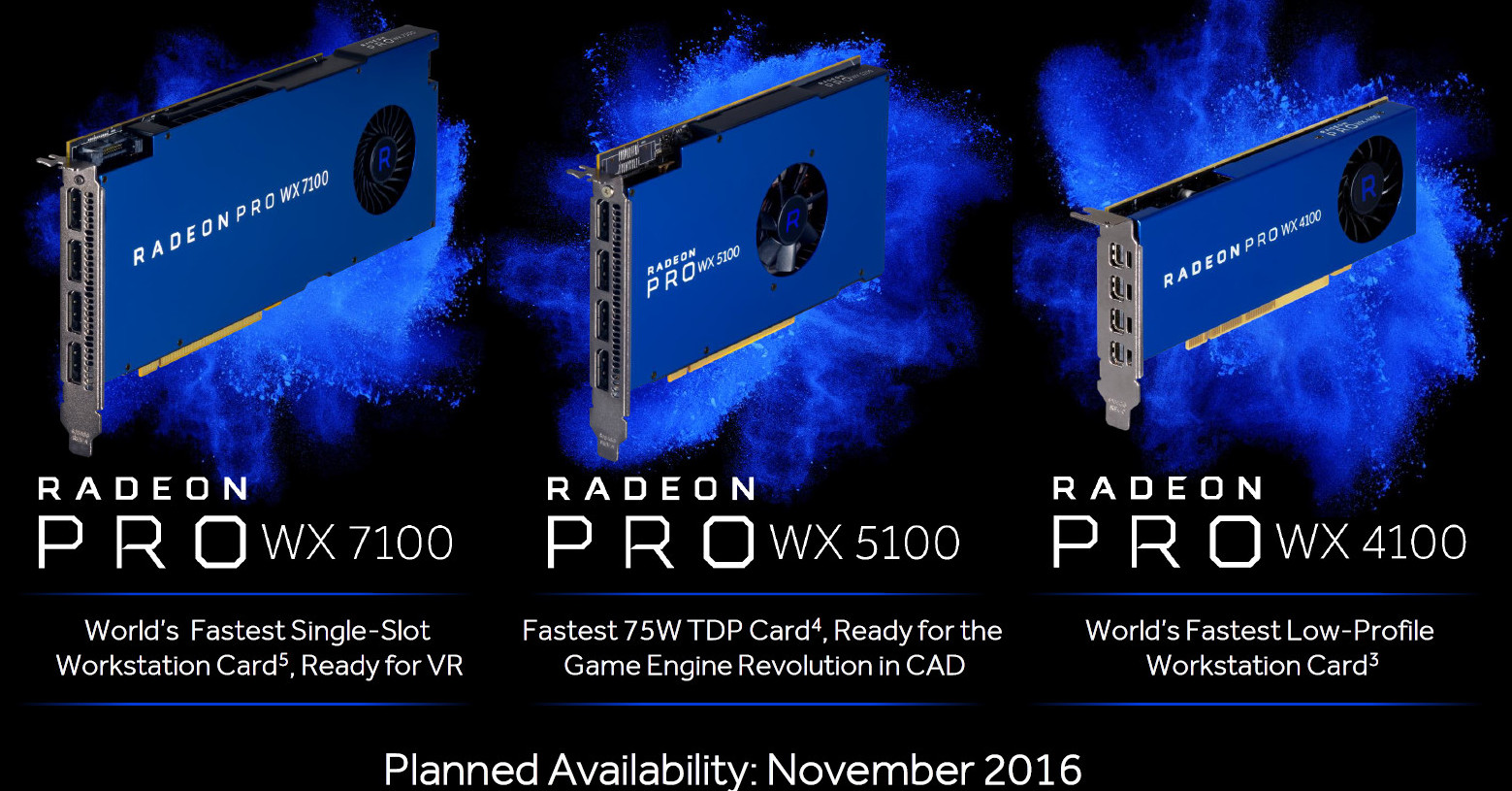
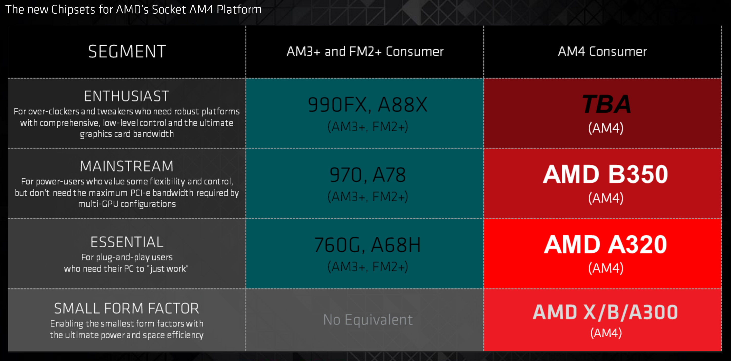
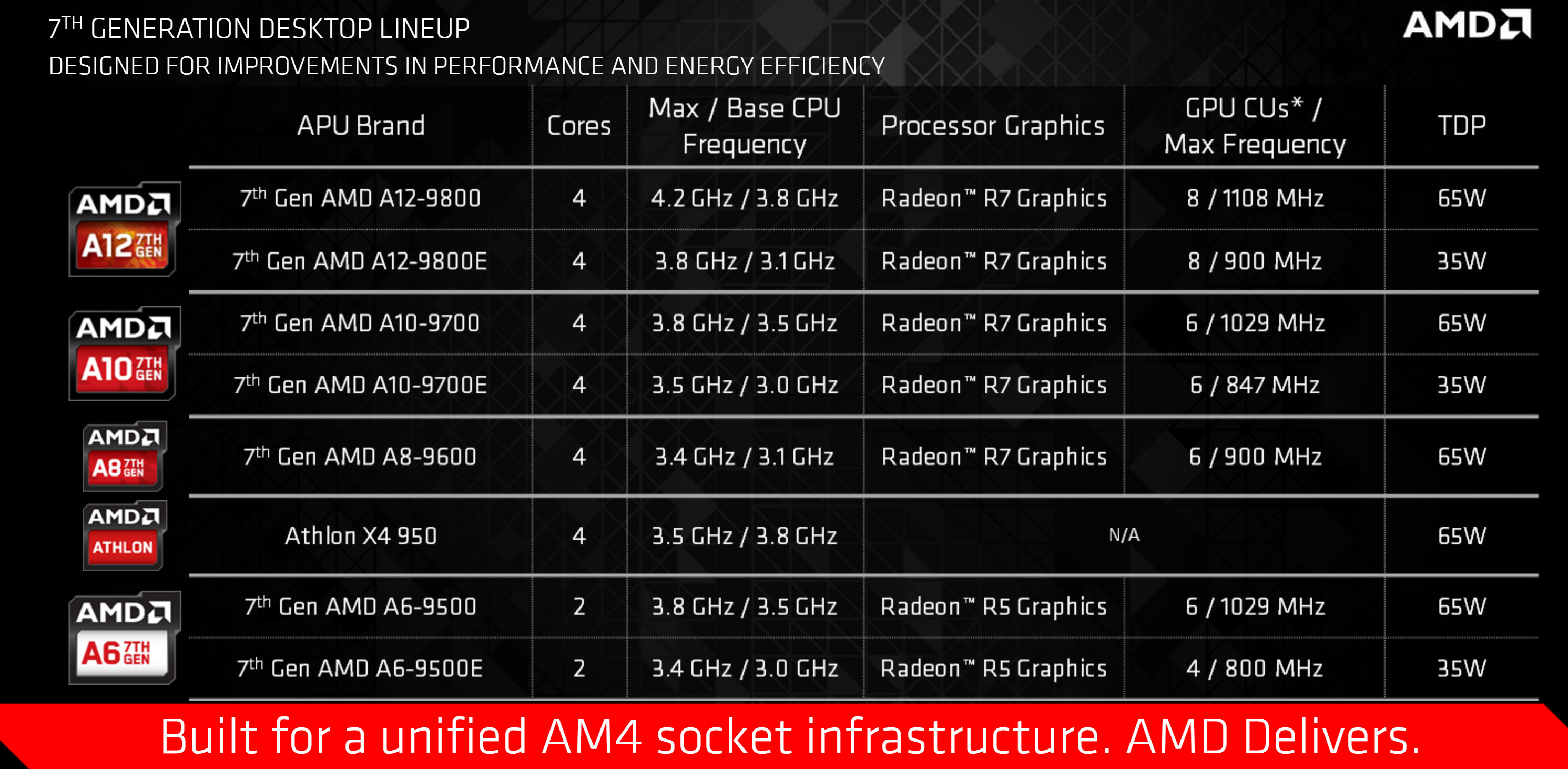
New AMD Radeon PRO W6000 Series Graphics Unleash High-Efficiency, Powerful CAD Performance for Mainstream Workstation Users

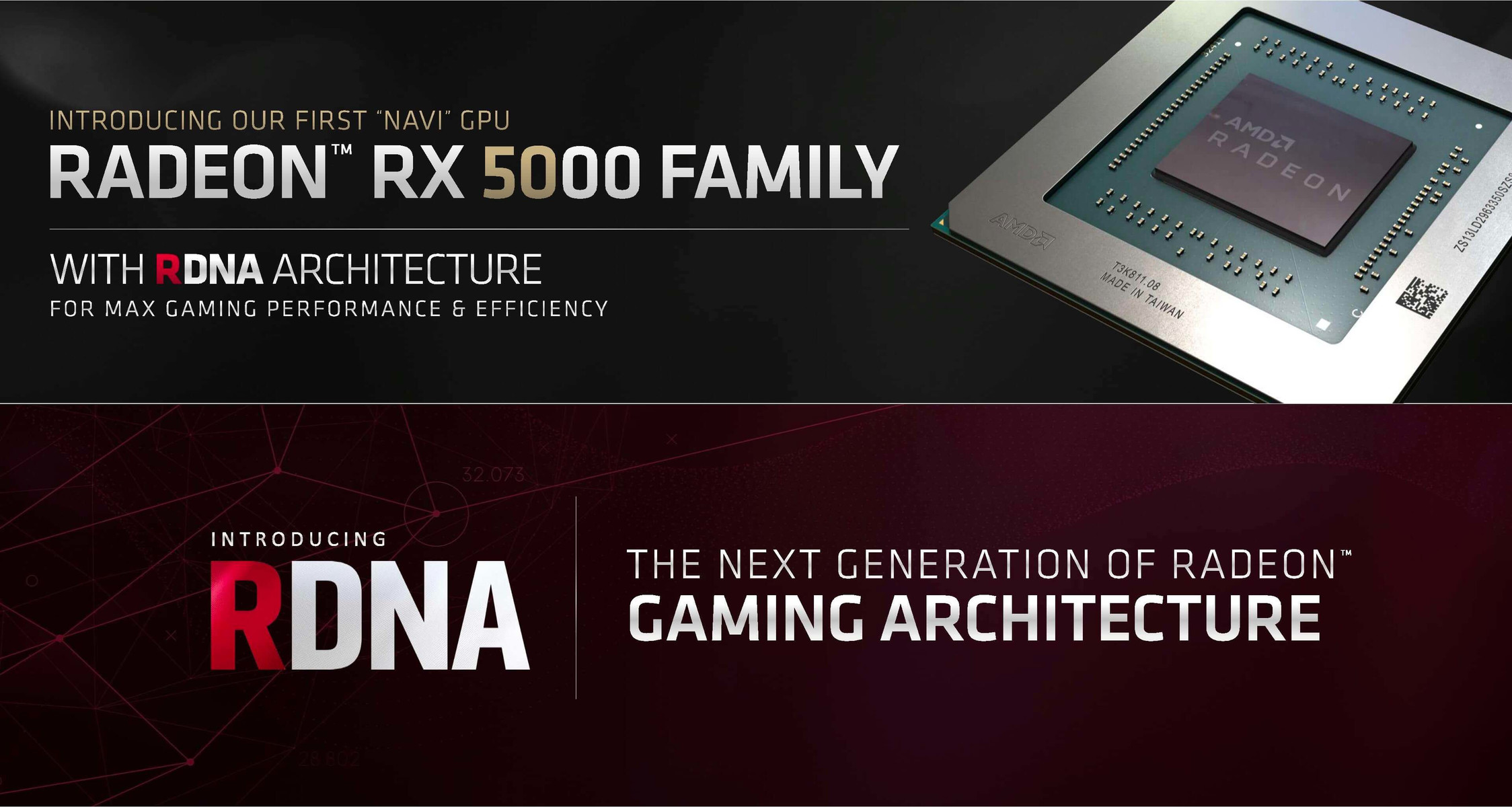
Today AMD announced new additions to the AMD Radeon PRO W6000 Series desktop and mobile workstation graphics lineup, designed to deliver exceptional performance, stability and reliability for professional users, including CAD designers, engineers and office knowledge workers. The new AMD Radeon PRO W6400 graphics card is built on the high-performance, energy efficient AMD RDNA 2 graphics architecture and advanced 6 nm manufacturing process technology, with 16 MB of high-bandwidth, low-latency AMD Infinity Cache memory technology acting as a bandwidth amplifier. Offering an ideal blend of performance and efficiency at an affordable price, the new graphics card is optimized for the requirements of today's popular CAD and office productivity applications in a compact design that can be easily added to modern small-form-factor desktops.

Compared to the previous generation, the AMD Radeon PRO W6400 graphics card delivers up to three times higher performance in Autodesk AutoCAD 2022 during 3D orbit rotational tests in shaded modes. It also offers up to 87 percent higher performance in McNeel Rhino using the Holomark 2 benchmark with mesh, object and model data stress tests. The new graphics card also offers performance gains in typical office applications and workloads, such as videoconferencing, email and web browsing, where reliability and stability are key. Additions to the AMD Radeon PRO product family also include the AMD Radeon PRO W6500M and AMD Radeon PRO W6300M GPUs for next-gen professional mobile workstations. The new GPUs are also built on AMD RDNA 2 graphics architecture with 6 nm process technology and harness up to 8 MB of AMD Infinity Cache memory technology to deliver ultra-high viewport frame rates, dependability and exceptional performance for professional applications.

MSI Announces Delta 15 and Alpha 15/17 AMD Advantage Laptops with Radeon RX 6000M Series Graphics

MSI, a world-leading gaming brand, announces the all-new AMD-powered gaming laptop, Delta 15 and the revamped Alpha 15/17, equipped with the AMD Ryzen 5000 H Series Mobile Processors and the up to latest AMD Radeon RX6700M Series Mobile Graphics. MSI continues to fulfill the diverse demand of gaming and leverage the strength in the AMD product line.

Delta 15 and Alpha 15/17 all come with the latest Radeon RX6000M Series Mobile Graphics, 1.5x faster performance compared to previous generations AMD graphics. * Powered by the AMD Radeon RX 6700M, Delta 15 provides ultra-high frame rates, while the Alpha 15/17, equipped with the AMD Radeon RX 6600M, delivers 1080p gaming at max settings.

Ten Years in, AMD to End Support for Radeon HD 7000, R200, R300 and Fury GCN Graphics Cards

AMD is ending support for the Radeon HD 7000 series, R200 series, R300 series, and R9 Fury series graphics cards, based on the oldest versions of the Graphics CoreNext architecture. The HD 7000 series debuted in 2011, R9 200 series in 2013, with the R9 300 series essentially being rebadged. The R9 Fury series joined the ranks in 2015. This would make the Radeon 21.5.2 the final drivers from these graphics cards, giving AMD the opportunity to clean-break its drivers from the RX 400 series "Polaris" and forward. A conclusion of driver support would mean that upcoming driver releases, including the 21.6.1 drivers released today, lack support for GPUs older than the RX 400 series. Should AMD encounter glaring security flaws with its drivers, it can, in the future, release special driver updates.

AMD Announces Radeon Pro W5700 Professional Graphics Card Based on "Navi"

AMD today announced the AMD Radeon Pro W5700, the world's first 7 nm professional PC workstation graphics card. It delivers new levels of performance and advanced features that enable 3D designers, architects and engineers to visualize, review and interact with their designs in real time, dramatically accelerating decision-making processes and product development cycles.

The AMD Radeon Pro W5700 workstation graphics card features the high-performance, energy-efficient AMD RDNA architecture and state-of-the-art GDDR6 memory to handle large models and datasets, and is the first PC workstation graphics card to support high-bandwidth PCIe 4.0 technology. It is ideal for professionals who push performance beyond traditional 3D design by generating photorealistic renders of their concepts and reviewing virtual prototypes of their designs in virtual reality (VR) environments.

AMD Radeon RX 5700 XT Confirmed to Feature 64 ROPs: Architecture Brief

AMD "Navi 10" is a very different GPU from the "Vega 10," or indeed the "Polaris 10." The GPU sees the introduction of the new RDNA graphics architecture, which is the first big graphics architecture change on an AMD GPU in nearly a decade. AMD had in 2011 released its Graphics CoreNext (GCN) architecture, and successive generations of GPUs since then, brought generational improvements to GCN, all the way up to "Vega." At the heart of RDNA is its brand new Compute Unit (CU), which AMD redesigned to increase IPC, or single-thread performance.

Before diving deeper, it's important to confirm two key specifications of the "Navi 10" GPU. The ROP count of the silicon is 64, double that of the "Polaris 10" silicon, and same as "Vega 10." The silicon has sixteen render-backends (RBs), these are quad-pumped, which work out to an ROP count of 64. AMD also confirmed that the chip has 160 TMUs. These TMUs are redesigned to feature 64-bit bi-linear filtering. The Radeon RX 5700 XT maxes out the silicon, while the RX 5700 disables four RDNA CUs, working out to 144 TMUs. The ROP count on the RX 5700 is unchanged at 64.

Rumor: AMD Navi a Stopgap, Hybrid Design of RDNA and GraphicsCoreNext

The Wheel of Rumors turns, and assumptions come and pass, sometimes leaving unfulfilled hopes and dreams. In this case, the rumor mill, in what seems like a push from sweclockers, places Navi not as a "built from the ground-up" architecture, but rather as a highly customized iteration of GCN - iterated in the parts that it actually implements AMD's RDNA architecture, to be exact. And this makes sense from a number of reasons - it's certainly not anything to cry wolf about.

For one, AMD's GCN has been a mainstay in the graphics computing world since it was first introduced back in 2012, succeeding the company's TeraScale architecture. Game engines and assorted software have been well optimized already to take advantage of AMD's design - even with its two ISAs and assorted improvements over the years. One of the most important arguments is derived from this optimization effort: AMD's custom designs for the console market employ architectures that are GCN-based, and thus, any new architecture that would be used by both Microsoft and Sony for their next-generation consoles would have to be strictly backwards compatible.

AMD Radeon RX 570 and China-specific RX 580 2048SP Based on Exact Same Chip

It's no news that AMD's Radeon RX 570 graphics card is carved out of the same "Polaris 20" silicon as the RX 580, by disabling 4 out of 36 GCN compute units. AMD kicked a controversy recently, when it launched a China-specific Radeon RX 580-branded SKU with the core-configuration of the cheaper RX 570, confusing Chinese consumers. It turns out that this RX 580 2,048 SP SKU is based on the same exact ASIC variant of the "Polaris 20" silicon as the RX 570, with the only difference being device ID.

We watch a lot of GamersNexus content. Our GPU Database curator noticed something interesting in their recent teardown of a Dataland Radeon RX 580 (2,048 SP) graphics card directly imported from China. The unique ASIC sub-variant code etched on the GPU's aluminium reinforcement brace matches that of the RX 570. AMD internally refers to the RX 570 as "Polaris 20 XL," and its ASIC code etched is supposed to be "215-0910052." For the RX 580, the real one, aka "Polaris 20 XTX," the code etched is "215-0910038." Thanks to GamersNexus' high-resolution filming, our curator was able to spot the ASIC code for "Polaris 20 XL" on the Dataland card's GPU. This confirms that AMD merely took an RX 570 and gave it a different device ID to create the RX 580 2,048 SP, leaving consumers to wade through the confusion.

AMD "Vega" Outsells "Previous Generation" by Over 10 Times

At its Computex presser, leading up to its 7 nm Radeon Vega series unveil, AMD touched upon the massive proliferation of the Vega graphics architecture, which is found not only in discrete GPUs, but also APUs, and semi-custom SoCs of the latest generation 4K-capable game consoles. One such slide that created quite some flutter reads that "Vega" shipments are over 10 times greater than those of the "previous generation."

Normally you'd assume the previous-generation of "Vega" to be "Polaris," since we're talking about the architecture, and not an implementation of it (eg: "Vega 10" or "Raven Ridge," etc.). AMD later, at its post event round-table, clarified that it was referring to "Fiji," or the chip that went into building the Radeon R9 Fury X, R9 Nano, etc., and comparing its sales with that of products based on the "Vega 10" silicon. Growth in shipments of "Vega" based graphics cards is triggered by the crypto-mining industry, and for all intents and purposes, AMD considers the "Vega 10" silicon to be a commercial success.

PSA: Flashing RX Vega 56 with RX Vega 64 BIOS Does Not Unlock Shaders

When TechPowerUp released GPU-Z v2.3.0 earlier this week, AMD Radeon RX Vega 56 users who had flashed their graphics cards with the video BIOS of the higher RX Vega 64, discovered that their stream processor count had shot up from 3,584 to higher counts under 4,096. Some of these users felt it more or less explained the performance jump experienced after the BIOS flash. Some users even saw wrong stream processor-counts of their untouched RX Vega 56 reference-design cards. TechPowerUp GPU-Z v2.3.0 incorrectly reports the stream processor count of flashed RX Vega 56 graphics cards, and some RX Vega 56 graphics cards out of the box; due to some under-the-hood bug in the way it reads the registers of AMD's new GPUs. We are working on an update to GPU-Z, which will fix this bug.

As we explained in our older article, flashing your RX Vega 56 with the BIOS of RX Vega 64 does not unlock stream processors, and the performance jump can be explained with the increased clock speeds. RX Vega 64 BIOS runs your RX Vega 56 reference-design graphics card at the higher reference clock speeds of 1247 MHz core, 1546 MHz boost, and 945 MHz memory; compared to the 1156/1471/800 MHz reference clocks of the RX Vega 56. This significant increase in clock speed is sufficient to explain the increased performance. Since the TMU count is tied to the number of GCN compute units visible to GPU-Z, the TMU count of certain RX Vega 56 cards is being incorrectly displayed. The upcoming update of GPU-Z addresses this as well.

AMD's Bristol Ridge APUs Released for the AM4 Platform in Retail Channels

AMD's AM4 socket really is shaping up to be one of the company's most versatile to date. From true quad-core CPUS (just now available through Ryzen 3's launch through to veritable svelte behemoths 8-core, 16-thread CPUs, AM4 has something for every consumer. AMD is now taking that show further with the release of the Bristol Ridge family of APUs, which includes eight APUs and three CPUs. While pricing wasn't announced at time of writing, the top-priced part should fall below the $110 mark and bottom out at $50, so as not to collide with AMD's Ryzen 3 1200 (although these products aren't specifically overlapping anyway.)

AMD's new entry-level processors will hit a maximum of 65 W TDP, with the top spot being taken by the 2-module, 4-threads A12-9800, running at 3.8 GHz base and 4.2 GHz Turbo. This part holds a Radeon R7 GPU with 512 Stream Processors (GCN 1.3, the same as in the Fury GPUs) running at 800 MHz Base and 1108 MHz Turbo. There are three 35 W parts (denoted by a capital E after the model name.) One thing users should take into account is that the Bristol Ridge APUs deliver a maximum of 8x PCIe 3.0 lanes - thus rendering a multi-GPU solution unfeasible.

AMD "Vega" Die-shot Revealed

AMD released the die-shot of its "Vega 10" ASIC. The multi-chip module (MCM) of the GPU die and two HBM2 memory stacks, sitting on a silicon interposer, is slightly smaller than the "Fiji" ASIC, as it features just two memory stacks. AMD didn't label the components of the GPU die, but we can make out 8 shader engines, holding 8 GCN compute units (CUs), each. This is unlike "Fiji," where the GPU holds four engines with 16 CUs, each. This would mean that each group of 8 CUs has its own dedicated geometry processor and rasterizer.

Since each CU holds 64 FP32 stream processors, we arrive at the total stream processor count of 4,096. Unlike "Hawaii," these stream-processors are FP16-capable, so simple compute tasks are handled at double the throughput. We also make out 32 render back-ends, double that of "Fiji" and "Hawaii," which could indicate 128 ROPs. The "Vega 10" ASIC features a 2048-bit HBM2 memory interface.

Update: AMD stated that the die-shot appeared in one of its marketing slides, but may not be real.

Biostar Intros the A6N-5100 "Kabini" Motherboard

Biostar introduced the A6N-5100 mini-ITX motherboard. A slight upgrade over the company's A6N-5000 from two years ago, the new board integrates AMD A4-5100 APU based on the "Kabini" silicon, which has the chops to outperform Intel's Celeron "Braswell" processors. The A4-5100 integrates a quad-core CPU ticking at 1.60 GHz, and AMD Radeon GCN graphics. The board features two DDR3 SO-DIMM slots, supporting up to 16 GB of memory, one PCI-Express 2.0 x16 slot, two USB 3.0 ports, HDMI display output, and storage connectivity that includes two SATA 6 Gb/s ports. The company didn't reveal pricing.

AMD Cripples Older GCN GPUs of Async-Compute Support?

AMD allegedly disabled asynchronous-compute technology support on older generations of Graphics CoreNext (GCN) architecture, since Radeon Software 16.9.2. With the newer drivers, "Ashes of the Singularity" no longer supports asynchronous-compute, a feature that improves performance in the game, on GPUs based on the first-generation GCN architecture, such as the Radeon R9 280X.

"Ashes of the Singularity" benchmarks run by Beyond3D forum members on GCN 1.0 hardware, comparing older drivers to version 16.9.2 shows that the game supports async-compute on the older drivers, and returns improved performance. AMD, on its part, is pointing users to a patch change-list from the developers of "Ashes..." which reads that the game supports DirectX 12 async-compute only on GCN 1.1 (eg: Radeon R9 290) and above.

AMD Reveals Three Entries on the WX Series Lineup: WX4100, WX5100 and WX7100

At its WX call, AMD focused on shifts in creativity from traditional design flows such as Solidworks, Adobe and Autodesk towards game engines as solutions for design visualization (Unreal Engine, Unity, CryEngine, or Autodesk's own Stingray platform), which signal changes in the creator ecosystem. Thanks to globalization, the Internet, and the available wealth of knowledge one can access through it, the line between amateurs and professionals is becoming more and more blurred. Now, those who would once be called amateurs are also using professional tools, and AMD plans to be at the forefront of technologies empowering creators to deliver their vision.

Radeon PRO serves to give creators more flexible and powerful solutions, leveraging open-source resources and centering the ecosystem back on creators and the tools they choose to use, with focused support on VR. As such, AMD is giving them the tools they need, by introducing three new products featuring the Polaris architecture, including 3 year standard + 7 year free extended warranty (including components such as the PCB itself, the PCI-Express slot, and the heatsinks), with AMD taking that extra 7 years as company commitment towards the quality of their products. Those three products are the WX4100, the WX5100, and the WX7100, and have planned, staggered availability throughout November.

Closer to the Metal: Shader Intrinsic Functions

Shader intrinsic functions stand as a partial solution for granting developers more control over existing computational resources and how they are leveraged. This capability (much touted by AMD as a performance-enhancing feature on their GCN-based products) essentially exposes features and capabilities that exist on the hardware developers are programming for, but wouldn't generally be able to access. This can happen either because they're being abstracted by a high-level API (Application Programming Interface, like DX11), or because the API isn't functionally able to access them. To understand why high-level APIs such as DX11 don't usually offer support for a piece of hardware's full feature list, or full processing capabilities, we must first look at the basic architecture of a given computer system.

AMD Unveils its 7th Generation A-Series Desktop APUs

AMD today unveiled its 7th generation A-series desktop APUs. Unlike its predecessors, the new chips are full-fledged SoCs, built in the new socket AM4 package, on which the company plans to launch its "Zen" processors. The 7th gen A-series APUs are based on the "Bristol Ridge" silicon, and are the first fully-integrated SoCs (systems-on-chip) from the company in the performance-desktop segment, in that the APU completely integrates the functionality of a motherboard chipset, including its FCH or southbridge.

This level of integration includes PCI-Express root-complex, USB 3.0, and storage interfaces such as SATA 6 Gb/s emerging directly from the AM4 socket. Some AM4 motherboards could still include a sort of "chipset," which expands connectivity options, such as USB 3.1 ports, additional SATA ports, and a few more downstream PCI-Express lanes. The amount of downstream connectivity and features decide the grade of the chipset. AMD is initially launching two chipsets, the A320 for the entry-level segment, and the B350 for mainstream desktops. The company plans to launch an even more feature-rich chipset at a later date (probably alongside ZEN "Summit Ridge" CPUs).

AMD Polaris 10 "Ellesmere" Die Shot Confirms Max Shader Count

An AMD Polaris 10 "Ellesmere" based graphics card (RX 470 or RX 480) was taken apart down to its die, for science. Close up die-shots of the silicon reveal that 36 GCN compute units is all that the silicon has, and that the RX 480 indeed maxes out this stream processor count, with 2,304 stream processors at its disposal.

The die is fabbed by GlobalFoundries, on its swanky new 14 nm FinFET process. Redditors good at pattern-recognition could make out 36 "structures" spread across four quadrants, deducing them to be the GCN compute units. Each of these CUs feature 64 stream processors. Roadmaps reveal that the next high-end GPUs by AMD could be based on its newer "Vega" architecture.

AMD Radeon RX 470 and RX 460 Official Specifications Leaked

The official specifications of two the two upcoming mainstream graphics cards by AMD, the Radeon RX 470, and the Radeon RX 460, were leaked to the web as slides from the company's official press presentation ahead of their early-August product launches. The RX 470 is based on the same "Ellesmere" Polaris10 silicon as the RX 480. It features 2,048 stream processors across 32 GCN compute units; 128 TMUs, 32 ROPs, and 4 GB of memory across a 256-bit wide GDDR5 memory interface.

The RX 470 features clock speeds of 926 MHz core, 1206 MHz boost, and 6.6 Gbps memory, working out to 211 GB/s memory bandwidth. The RX 460, on the other hand, is based on the "Baffin" Polaris11 silicon, featuring 896 stream processors, 48 TMUs, 16 ROPs, and 4 GB of memory across a 128-bit wide GDDR5 memory interface. Its core is clocked at 1090 MHz, with 1200 MHz boost, and 7 Gbps memory, working out to 112 GB/s memory bandwidth. The RX 470 draws power from a single 6-pin PCIe power connector as its TDP is rated at 120W; the RX 460 relies entirely on the PCIe slot for its power, as its TDP is rated at <75W. The RX 470 will be available from 4th August, 2016; with the RX 460 following on 8th August.

AMD Radeon RX 470 and RX 460 Specifications Confirmed

AMD confirmed specifications of its second and third "Polaris" architecture graphics cards in a leaked presentation, the Radeon RX 470, and the Radeon RX 460. The RX 470 will be AMD's attempt at a graphics card that plays everything at 1080p resolution, under $150. The Radeon RX 460, on the other hand, is based on the new 14 nm Polaris11 "Baffin" silicon, and could be ideal for MOBA games with light GPU requirements.

The Radeon RX 470 is carved out from the Polaris10 "Ellesmere" silicon that the RX 480 is based on, it features 2,048 stream processors across 32 GCN compute units, 128 TMUs, 32 ROPs, and a 256-bit wide GDDR5 memory interface, holding 4 GB of memory. The card draws power from a single 6-pin PCIe power connector. The Radeon RX 460, on the other hand, features 896 stream processors across 14 compute units, 2 GB of GDDR5 memory across a 128-bit wide memory interface, and relies on the PCI-Express slot entirely for power. The reference RX 460 board looks quite similar to the Radeon R9 Nano, but features a simpler spiral heatsink under the fan. Despite rumors to the contrary, it looks like Vega is on-course for a 2017 launch after all.

AMD Radeon RX 480 Graphics Card Now Available

AMD today announced availability of its Radeon RX 480 graphics card. The card is currently only available in its 8 GB variant, with the more cost-effective 4 GB variant touting the magic price-tag of $199 slated for July. The 8 GB variant being launched today will start at $229. Based on the 14 nanometer Polaris 10 silicon, the RX 480 takes advantage of the 4th generation Graphics CoreNext (GCN) architecture.

The chip features 2,304 stream processors spread across 36 GCN compute units, 144 TMUs, 32 ROPs, and a 256-bit GDDR5 memory interface, holding 8 GB of memory. At its given clock speeds, the card features 256 GB/s of memory bandwidth, although AMD claims DCC memory compression technology to effectively increase memory bandwidth by up to 30 percent in the best case scenarios. The core ticks at 1266 MHz, and the memory at 8 GHz (GDDR5-effective). The card features a TDP of just 150W, and draws power from a single 6-pin PCIe power connector. Display outputs include three DisplayPort 1.4 and one HDMI 2.0b. Custom-design cards could feature DVI connectors.

Read the TechPowerUp Reviews of this card: AMD Radeon RX 480 8GB | AMD Radeon RX 480 CrossFire

AMD Confirms Key "Summit Ridge" Specs

AMD CEO Lisa Su, speaking at the company's Computex reveal held up the most important CPU product for the company, the new eight-core "Summit Ridge" processor. A posterboy of the company's new "Zen" micro-architecture, "Summit Ridge" is an eight-core processor with SMT enabling 16 threads for the OS to deal with, a massive 40% IPC increase over the current "Excavator" architecture, and a new platform based around the AM4 socket.

The AM4 socket sees AMD completely relocate the core-logic (chipset) to the processor's die. Socket AM4 motherboards won't have any chipset on them. This also means that the processor has an integrated PCI-Express gen 3.0 root complex, besides the DDR4 integrated memory controller. With the chipset being completely integrated, connectivity such as USB and SATA will be routed out of the processor. The AM4 socket is shared with another kind of products, the "Bristol Ridge" APU, which features "Excavator" CPU cores and a 512-SP GCN 1.2 iGPU.

AMD Polaris 10 "Ellesmere" as Fast as GTX 980 Ti: Rumor

At a presser in Taiwan for its Radeon Pro Duo launch, AMD talked extensively about its upcoming "Polaris" and "Vega" family of GPUs. The company appears to be betting heavily on two SKUs it plans to launch this June, Polaris 10 and Polaris 11. Polaris 10 is an internal designation to Radeon R9 490(X), based on the 14 nm "Ellesmere" silicon. It may be the biggest chip AMD builds on the "Polaris" architecture, but it won't exactly be a "big chip," in that it doesn't succeed "Fiji." That honor is reserved for "Vega," which debuts in early-2017.

The "Ellesmere" silicon is more of AMD's competitor to NVIDIA's GP104. It is rumored that the R9 490(X), based on this silicon, will offer consumers performance rivaling the GeForce GTX 980 Ti (ergo faster than the Radeon R9 Fury X), at a USD $300-ish price point. "Ellesmere" will be a lean-machine, physically featuring up to 2,560 4th generation GCN stream processors (2,304 enabled on Polaris 10), a possible 256-bit GDDR5X memory interface, and a deep sub-200W typical board power rating.

AMD "Greenland" Vega10 Silicon Features 4096 Stream Processors?

The LinkedIn profile of an R&D manager at AMD discloses key details of the company's upcoming "Greenland" graphics processor, which is also codenamed Vega10. Slated for an early-2017 launch, according to AMD's GPU architecture roadmap, "Greenland" will be built on AMD's "Vega" GPU architecture, which succeeds even the "Polaris" architecture, which is slated for later this year.

The LinkedIn profile of Yu Zheng, an R&D manager at AMD (now redacted), screencaptured by 3DCenter.org, reveals the "shader processor" (stream processor) count of Vega10 to be 4,096. This may look identical to the SP count of "Fiji," but one must take into account "Greenland" being two generations of Graphics CoreNext tech ahead of "Fiji," and that the roadmap slide hints at HBM2 memory, which could be faster. One must take into account AMD's claims of a 2.5X leap in performance-per-Watt over the current architecture with Polaris, so Vega could only be even faster.

AMD Announces Exciting DirectX 12 Game Engine Developer Partnerships

AMD today once again took the pole position in the DirectX 12 era with an impressive roster of state-of-the-art DirectX 12 games and engines, each with extensive tuning for the Graphics Core Next (GCN) architecture at the heart of modern Radeon GPUs.

"DirectX 12 is poised to transform the world of PC gaming, and Radeon GPUs are central to the experience of developing and enjoying great content," said Roy Taylor, corporate vice president, Content and Alliances, AMD. "With a definitive range of industry partnerships for exhilarating content, plus an indisputable record of winning framerates, Radeon GPUs are an end-to-end solution for consumers who deserve the latest and greatest in DirectX 12 gaming."

AMD Takes 83% Share of Global VR System Market

AMD announced today at the 2016 Game Developer Conference that the company will underscore its dominance of the global virtual reality systems market. It revealed new advances in hardware and software to further the reach of VR, and unveiled its new GPU certified program that simplifies adoption of VR technology for consumers and content creators.

"AMD continues to be a driving force in virtual reality," said Raja Koduri, senior vice president and chief architect, Radeon Technologies Group, AMD. "We're bringing the technology to more people around the world through our efforts to expand the VR ecosystem with VR i-Cafés in China, new Oculus Rift and HTC Vive headsets, and a wide variety of content partners in gaming, entertainment, education, science, medicine, journalism and several other exciting fields."

AMD is also making VR more easily accessible to consumers and content creators with its GPU certified program featuring the new "Radeon VR Ready Premium" and "Radeon VR Ready Creator" tiers. Its forthcoming Polaris GPUs and award-winning AMD LiquidVR technology will simultaneously advance groundbreaking VR-optimized graphics.
Return to Keyword Browsing
Apr 25th, 2024 13:01 EDT change timezone

New Forum Posts

Popular Reviews

Controversial News Posts