News Posts matching #GF100

Return to Keyword Browsing

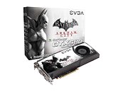
EVGA Intros GeForce GTX 580 Batman: Arkham City Graphics Card

EVGA released a new Batman: Arkham City-themed GeForce GTX 580 graphics card. Carrying the model number 015-P3-1582-A1, this card carries NVIDIA clock speeds of 797/1594/4050 MHz (core/CUDA cores/memory effective). Apart from the game-themed cooler shroud sticker and a themed box, we can't really see what's new with this product. Perhaps it has a voucher for a copy of the game?

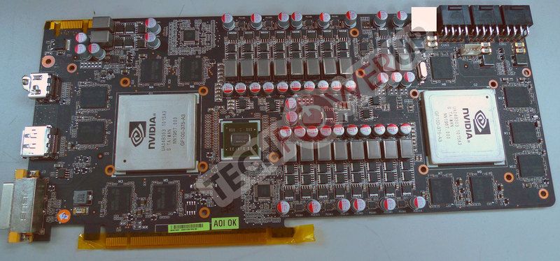
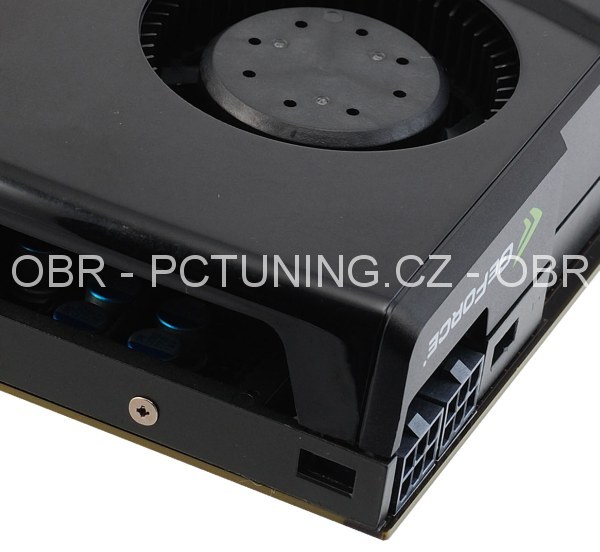
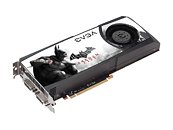
Based on the 40 nm GF100 graphics processor, GeForce GTX 580 is the single fastest GPU on the planet. It packs 512 CUDA cores, and 1536 MB of GDDR5 memory across a 384-bit wide memory bus. The GTX 580 also packs features Batman: Arkham City can benefit from, such as PhysX. Available on American retailer Newegg.com, the EVGA GTX 580 Batman: Arkham City Edition is priced at $529.99. At $30 over the base model GTX 580, it has got to pack a copy of the game.

Arctic Intros Accelero Mono Plus VGA Cooler

Arctic released a new VGA cooler, the Accelero Mono PLUS. This cooler can handle thermal loads of up to 200W, and maintains a compact fin-stack design, unlike the monolitic heatsink design of the Accelero L2 series. Measuring 136 (L) x 138 (W) x 51 (H) mm, its main heatsink weighs 348 g. From an exposed-copper base (with pre-applied adhesive thermal compound) arise five 6 mm thick copper heat pipes, that fan out to pass through an aluminum fin stack. This stack is ventilated by a 120 mm PWM-controlled fan that can spin at speeds between 400 and 1500 RPM. It can be as quiet as 0.4 Sone.

MSI Sells Twin Frozr II VGA Cooler Loose in Japan

MSI's engineers struck gold with their Twin Frozr II cooler design, introduced a couple of generations of GPUs ago. Twin Frozr II soon became MSI's workhorse VGA cooler for high-end non-reference design graphics cards, on both the NVIDIA and ATI/AMD lines. It is reported that MSI is now selling this VGA heatsink loose in the Japanese market, so you don't have to buy an new MSI graphics card, and just upgrade your existing one with it.

This variant of Twin Frozr II has GPU retention hole layout that matches that of GF100 and GF110-based single-GPU graphics cards, i.e. GTX 465, GTX 470, GTX 480, GTX 570, and GTX 580. The cooler measures 251.9x100.9x35 mm, weighing 520 g. It consists of a nickel-plated copper base, from which five heat pipes (6 mm thick pipes towards the central portion of the base, 8 mm thick towards periphery) originate, conveying heat to a large aluminum fin stack. This stack is ventilated by two PWM-controlled fans. The Twin Frozr II is priced at ¥5,980 or US $73.

NVIDIA GeForce GTX 580 Reference Design Graphics Card Pictured

Here are the first pictures of what is touted to be the GeForce GTX 580 reference design graphics card by NVIDIA, by sections of the Chinese media. There are some interesting inferences that can be drawn just by the looks of the card. To begin with the cooler bears an uncanny resemblance to one of the earliest design iterations of the GeForce GTX 480 (pictured here and here). In its final iteration, NVIDIA gave the GTX 480 a more massive cooler, perhaps to keep up with its finalized clock speeds. If the design of the GTX 580 cooler is anything to go by, it means that either NVIDIA refined the GF100 architecture in the GF110 (on which GTX 580 is based) a great deal, increasing performance per Watt; or that since GTX 580 is in its development stage, its final version could look different. GeForce GTX 580 is being designed as a counter to AMD's Radeon HD 6900 series single-GPU graphics cards that are based on the new Cayman graphics core, which is slated for release in late November. It is expected to be 20% faster than the GTX 480.

Zotac Designs GeForce GTX 460 X2 Graphics Card

Zotac is another NVIDIA partner who isn't pleased that the GeForce GTX 480 isn't holding performance leadership, but has the engineering potential to outdo it. Earlier in June, Galaxy showed off a dual Fermi graphics card that makes use of two GF100 graphics processors in the GeForce GTX 465 configuration. Zotac waited for a more mature implementation of the Fermi architecture, found out that the GF104-based GeForce GTX 460 isn't lacking much in performance compared to the GTX 465, with vastly better thermal specifications, and went on to design its latest high-end card, which it now refers to as the Zotac GeForce GTX 460 X2. The card makes use of two GeForce GTX 460 1 GB GPUs in an internal SLI, much like every other dual-GPU NVIDIA card.

The card uses an NVIDIA nForce 200 bridge chip to semaphore and broadcast data between the two GPUs, a dual 3+1+1 phase VRM that draws power from two 8-pin PCI-E power connectors, and display connectivity is relayed to the rear-panel from both the GPUs, that's four dual-link DVI, and one mini-HDMI. What this also means is that with just this one card, you can use the 3D Vision Surround feature, while retaining SLI multi-GPU scaling. If that's not all, there's a SLI connector, which lets you pair this with another card of its kind, for GTX 460 Quad-SLI. Zotac is yet to finalize a cooling solution to suit it best. GF104 could be NVIDIA's easiest route to a dual-GPU graphics card that establishes performance leadership. The GF104 physically has 384 CUDA cores (336 on Zotac's card, since it's in the GTX 460 configuration), and has shown to be capable of high GPU/Shader clock speeds. More details about Zotac's card are awaited.

Arctic Intros Accelero Xtreme Plus VGA Cooler, Supports GF100-based Graphics Cards

Arctic Cooling silently introduced the Accelero Xtreme Plus VGA cooler. Built as an extension of the same essential design of the Accelero Xtreme, the Accelero Xtreme Plus supports the latest NVIDIA GF100-based graphics cards, such as GeForce GTX 480, GTX 470, GTX 465. The main heatsink is designed to handle thermal loads of up to 250W. The cooler is also compatible with the mounting plates of older some Accelero models that give it compatibility with other popular GPUs, importantly support for Radeon HD 5000 and GeForce 9/GTS 200 series with the VR001 mounting kit.

The main heatsink consists of a copper-made GPU contact base from which five heat pipes convey heat to two blocks of aluminum fins that are cooled by three 92 mm fans. A patented cooler shroud design works to dampen noise generated by the three fans. The three fans spin at speeds between 800 and 2,000 rpm. The heatsink measures 290 L x 104 W x 56 H mm, weighing 622 g. Included in the package apart from the main heatsink are heatsinks for the memory chips and VRM. The Arctic Accelero Xtreme Plus is priced at US$ 65.95 or 54,95 €.

Sparkle Announces Calibre GTX 480 Graphics Card with Custom Cooling Solution

SPARKLE Computer Co., Ltd., the professional VGA card manufacturer and supplier, today proudly announced the Calibre X480 graphics card, equipped with the Accelero Xtreme Cooling Solution from Arctic Cooling, providing the world's fastest DX11 performance to gamers unbeatable cooling effects.

The Calibre X480 Graphics Card brings a host of the next generation of gaming architecture GF100--including tessellation, Direct Compute and all other DirectX 11 hardware features. GF100 architecture is specifically designed to support next generation gaming effects such as ray tracing, order-independent transparency, and fluid simulations. By using GF100 architecture, the Calibre X480 Graphics Card gets a tremendous boost in DX11 game performance and image quality, and brings film-like game characters and objects to users. GF100 architecture also enhances PhysX simulations with tremendous speed upgrade. In addition, GPU computing now can be put in practice in latest DX11 games for improve DX11 gaming efficiency.

GF100 512 Core Graphics Card Tested Against GeForce GTX 480

NVIDIA seems to have overcome initial hiccups with the GF100 graphics processor, and could release a new graphics card that makes use of all 512 CUDA cores, and 64 TMUs on the GPU. The GeForce GTX 480 was initially released as a top SKU based on the GF100, with 480 out of the 512 CUDA cores enabled. What NVIDIA calls the new SKU is subject to some speculation. While GPU-Z screenshots show that the 512 core model has the same device ID (hence the same name, GeForce GTX 480), leading us to believe that this is a specifications update for the same SKU à la GeForce GTX 260 (216 SP), it seems possible that the release-grade models could carry a different device ID and name.

Expreview carried out a couple of tests on the 512 core "GTX 480" graphics card, and compared it to the 480 core model that's out in the market. NVIDIA GeForce 258.96 drivers were used. The 512 core card got a GPU Score of 10,072 points compared to 9,521 points of the 480 core card, in 3DMark Vantage Extreme preset. The additional TMUs showed an evident impact on the texture fillrate, 41.55 GTexel/s for the 512 core card against 38.82 GTexel/s for the 480 core card.

ASUS Working on MARS II Dual GTX 480 Graphics Accelerator

After treating the enthusiast community to the Republic of Gamers (ROG) ARES Dual HD 5870 graphics accelerator, ASUS isn't wasting any time is designing its successor, referred to (for now) as "MARS II". This graphics accelerator uses two NVIDIA GeForce GTX 480 (GF100) GPUs on one board, that's right, the first dual-GPU accelerator based on GF100, which is dreaded for its thermal and electrical characteristics so much, that NVIDIA is content with having the second-fastest graphics card in the market (GTX 480), with no immediate plans of working on a dual-GPU accelerator.

ASUS' ambitious attempt is in the design stage deep inside its R&D, where the design is in an evaluation state. The R&D gave us some exclusive pictures of the MARS II PCB to treat you with. To begin with, the card's basic design is consistent with almost every other dual-GPU NVIDIA card in recent past. There are two independent GPU systems, each with its own VRM and memory, which are interconnected by an internal SLI, and connected to the system bus by an nForce 200 bridge chip. On this card, two GF100 GPUs with the same configuration as GeForce GTX 480 (GF100-375-A3) are used, each having 480 CUDA cores, and connecting to 1536 MB of GDDR5 memory across a 384-bit wide memory interface.

New NVIDIA GF100 Board Surfaces, Suggests New High-End SKU

Sources in the hardware industry leaked some interesting pictures of a new, supposedly reference-design NVIDIA GF100 GPU graphics card PCB, watermarked by board partner Little Tiger. The pictures reveal a PCB that's similar to that of the GeForce GTX 480, but with a stronger VRM that makes use of better high-C surface-mount capacitors (completely doing away with cylindrical capacitors), and draws power from two 8-pin PCI-Express power inputs. The design can deliver up to 375W of power (that's not the board power we're talking about).

This also opens up speculation about what NVIDIA would do with this design. The most talked about theory as of now points to a new high-end SKU by NVIDIA based on the GF100, that enables all streaming multiprocessors (SMs) physically present on the GF100, taking the CUDA core count up to 512, and ROP count to 64. The most likely marketing name for this SKU is GeForce GTX 485. Apart from higher CUDA core and ROP count than that of the GTX 480, slightly higher clock-speeds for the GPU are also on the cards. The memory subsystem remains untouched, at 1536 MB of GDDR5 memory clocked at 924 MHz (effective 3.7 GHz), over a 384-bit wide memory interface. NVIDIA could release this SKU this fall.

Galaxy Readies Dual-Fermi Graphics Card

Galaxy is finally breaking ground on graphics cards with two GF100 "Fermi" GPUs from NVIDIA, with the company displaying one such design sample at the ongoing Computex event. The dual-Fermi board uses essentially the same design NVIDIA has been using for generations of its dual-GPU cards, involving an internal SLI between two GPUs, which connect to the system bus via an nForce 200 bridge chip, and are Quad SLI capable.

The power conditioning and distribution on this design consists of two sets of 4+1 phase VRM, the card draws power from two 8-pin PCI-Express power connectors. The GPUs carry the marking "GF100-030-A3", which indicates that it has the configuration of GeForce GTX 465, and since we count 8 memory chips per GPU system with no traces indicative of the other two memory chips per GPU sitting on their own memory channels, on the reverse side of the PCB, it is likely that the GPUs have a 256-bit wide memory interface. Galaxy, however, calls the card GTX 470 Dual. Output connectivity includes 3 DVI-D, with a small air-vent. It's likely that the cooler Galaxy designs will dissipate hot air around the graphics card, rather than out through the rear-panel.

Gigabyte Rolls Out Twin-Fan GeForce GTX 465

Gigabyte rolled out its first graphics card based on NVIDIA's newest GPU, the GeForce GTX 465. The card features Gigabyte's own design, which makes use of the Ultra Durable VGA construction, a combination of PCB with 2 oz thick copper layers, Japanese solid-state capacitors, grade 1 memory chips, ferrite-core chokes and low RDS on MOSFETs. The cooler uses a large aluminum fin block which is cooled by two 80 mm fans. Though geared for overclocking, the card comes with NVIDIA reference clock speeds of 607/1215/3206 MHz (core/shader/memory). The GTX 465 SKU is derived from the GF100 die, it features 352 CUDA cores, and 1 GB of GDDR5 memory across a 256-bit wide interface. It is priced at a standard $279.

NVIDIA Releases GeForce GTX 480M, World's Fastest Notebook GPU

NVIDIA made its GeForce GTX 480M GPU official today. The DirectX 11 compliant GPU is based on the GF100 core and packs all the features of its desktop counterpart, such as decentralized hardware tessellation, next-generation CUDA and DirectCompute 5.0. The GF100 core has a configuration similar to the GeForce GTX 465 desktop GPU. It has three of its four graphics processing clusters (GPCs), and 11 out of 16 streaming multiprocessors (SMs) enabled, giving a CUDA core count of 352. To reduce the overall board footprint, the GPU makes do with a 256-bit wide GDDR5 memory interface, with 1 GB of memory.

To make keep up with the electrical constraints of notebooks, the GTX 480M uses much lower clock-speeds than any desktop product that uses GF100. The core is clocked at 425 MHz, shader domain at 850 MHz, and memory at 600 MHz (real) or 2.40 GHz (effective), which gives a memory bandwidth of 76.8 GB/s. As mentioned earlier, the full feature-set of its desktop counterparts is packed with the GTX 480M, including support for NVIDIA 3D Vision, PureVideo HD, PhysX, and CUDA. It can pair with up to two boards of its kind in 2-way SLI. Constraints of the notebook form-factor won't allow any more boards, anyway. The GPU is open to Notebook manufacturers to plan their designs around. NVIDIA claims the GTX 480M to be the fastest notebook GPU. It finds direct competition in the ATI Mobility Radeon HD 5870, which is based on the 800 stream processor-laden Juniper core.

MSI Readies Twin Frozr II Based GeForce GTX 400 Series Graphics Cards

MSI is readying three new non-reference design graphics cards based on the entire series of GeForce GTX 400 series GPUs, including the upcoming GeForce GTX 465. The new cards will make use of the company's tried and tested Twin-Frozr II GPU cooler to keep the scorching GF100 GPU running. Unlike Twin Frozr II coolers used on ATI Radeon HD 5800 series GPUs, which have bases with heat pipes making direct contact with the GPU, in its GF100 implementation, the cooler will have large copper bases to quickly transfer heat from the GPU to the cooler. Perhaps MSI's mention of "high density" could also indicate that it would have more aluminum fins. The 8 mm thick heat pipes, which MSI refers to as SuperPipes, stay on. The SKUs will likely be called the MSI N480/N470/N465 Twin Frozr II, for models with the GeForce GTX 480, GTX 470, and GTX 465, respectively.

TechPowerUp GPU-Z 0.4.3 Released

TechPowerUp rolled out a new version of GPU-Z, the popular graphics sub-system diagnostic utility. Version 0.4.3 comes with a load of new features and stability updates. Highlights include full capability to monitor voltages on the GeForce GTX 480, a new method of voltage monitoring which extends support for many ATI and NVIDIA graphics cards, support for the upcoming GeForce GTX 465, GT 320M GT 335M, ION variant, GT 340, Tesla C2050, Tesla M2050, and other Quadro series GPUs, new display languages including Spanish and Hungarian, among other stability updates.

DOWNLOAD: GPU-Z 0.4.3

Change log follows.

Galaxy Readies Single-Slot GeForce GTX 470 Graphics Card

Galaxy is working on a single-slot graphics card based on the GF100 in its GeForce GTX 470 version. If that didn't boggle your mind, the fact that it's not another card with a water-block, but a single-piece air-cooled card surely will. Enter the Galaxy GTX 470 model known as "Katana" in Japan and "Razor" in other markets. The PCB appears to be a little over 10 inches long, looks-wise makes use of Galaxy's Blue-silver-copper scheme from its other non-reference GTX 470 GC card.

The single-slot air cooler covers the entire length of the PCB, with a fan that draws air from both sides of the PCB, and has grills that reveal the cooler's internal network of copper air-channels, and a slab of copper that is spread across most of the PCB's area that holds the GPU and memory. The cooler makes use of vapour-chamber technology. The card draws power from 8-pin and 6-pin power connectors. It is 4-way SLI capable. It is expected that the card comes with at least NVIDIA reference clock speeds, all other specifications remain the same: 448 CUDA cores, 1280 MB of GDDR5 memory across 320-bit interface, and connectivity which includes two DVI-D and a mini HDMI. It is expected to deck up Galaxy's Computex booth.

NVIDIA Designs GeForce GTX 460

NVIDIA is said to be working on another GF100-based SKU, which further cuts down from the GeForce GTX 470. The new SKU, GeForce GTX 460, is expected to rival ATI Radeon HD 5850 in the sub-$300 market segment. The GF100 will be configured to have a 256-bit wide GDDR5 memory interface, driving 1024 MB (1 GB) of memory. Clock speeds could be another thing NVIDIA uses as the determining factor. The GTX 460 will not have a reference design as such, and AIC partners will be allowed to release their own designs from day one. The new SKU is expected to release in June. Pictured below is the GTX 470 PCB.

Thermalright Makes its Popular VGA Coolers Fermi-Ready

Thermalright is said to be working on a bolt-through kit (BTK), the GF 100 VGA BTK, that lets popular existing VGA heatsinks by the company to support the NVIDIA GF100 GPU, on GeForce GTX 480 and GeForce GTX 470 graphics cards. The Thermalright Spitfire, HR-03 GT and HR-03 GTX heatsinks will be able to make use of the new BTK. The company is also said to be working on two new VRM heatsinks that are tailor-made for the reference PCBs of the two cards, the VRM GTX 480, and VRM GTX 470. These allow existing users of the above three heatsinks, and people looking to buy them some future-proofing. The GF 100 VGA BTK, VRM GTX 480 and VRM GTX 470 will be released in the weeks to come.

NVIDIA Announces the GeForce GTX 480 and GeForce GTX 470 Graphics Cards

NVIDIA finally released the graphics cards it made many wait for: the DirectX 11 compliant GeForce GTX 480 and GeForce GTX 470. The two were unveiled at the PAX East gaming event, in the United States, as publications were allowed to post reviews right away. The two are based on the NVIDIA GF100 GPU, built on the 40 nm process. The higher-end GeForce GTX 480 packs 480 shader units (now referred to by NVIDIA as "CUDA cores"), branched geometry processing along with multiple tessellation units, and a 384-bit wide GDDR5 memory interface to connect to 1536 MB (1.5 GB) of memory.

The GeForce GTX 470 is the more affordable part, it packs 448 CUDA cores, and a 320-bit GDDR5 memory interface to connect to 1280 MB (1.25 GB) of memory. Both models support new features by NVIDIA, such as CUDA 3.0, faster PhysX acceleration, Stereoscopic 3D, 3D Vision surround multi display technology, as well as support for OpenCL and DirectCompute 5.0. While the GeForce GTX 480 has a suggested retail price of US $499, the GTX 470 is suggested to be priced at $349, although final pricing set by board partners could vary. NVIDIA is initially making tens of thousands of these cards, which should be available worldwide a little after April 12th.

NVIDIA Preparing First Fermi-Derivative Performance GPU, GF104

With the launch of GeForce GTX 400 series enthusiast-grade graphics cards based on the GF100 GPU being a stone's throw away, it is learned that work could be underway at NVIDIA to develop a new performance GPU as a successor to G92 and its various derivatives, according to 3DCenter.org, a German tech portal. Codenamed GF104, the new GPU targets performance/price sweet-spots the way G92 did back in its day with the GeForce 8800 GT and 8800 GTS-512, which delivered high-end sort of performance at "unbelievable" price points. The GF104 is a derivative of the Fermi architecture, and uses a physically down-scaled design of the GF100. It is said to pack 256 CUDA cores, 32 ROPs, 32 TMUs, and a 256-bit wide GDDR5 memory interface. The more compact die as a result could achieve high clock speeds, like G92 did compared to the G80.

GF104 is believed to form three SKUs to fill performance-thru-mainstream market segments, starting with the fastest GeForce GTS 450, GeForce GTS 440, and GeForce GTS 430 (likely name). Among these, the GTS 450 enables all of GF104's features and specifications, with well over 700 MHz core speed, 1500 MHz shader, and 1800 MHz memory. This part could be priced at around the 240 EUR mark, and target performance levels of the ATI Radeon HD 5830. A notch lower, the GTS 440 has all the hardware inside the GF104 enabled, but has around 20% lower clock speeds, priced over 160 EUR, under 180 EUR. At the bottom is the so-called GTS 430, which could disable a few of the GPU's components, with 192 CUDA cores, and 192-bit GDDR5 memory interface, priced under $150. The lower two SKUs intend to compete with the Radeon HD 5700 series. The source says that the new SKUs could be out this summer.

NVIDIA Claims Upper Hand in Tessellation Performance

A set of company slides leaked to the press reveals that NVIDIA is claiming the upper hand in tessellation performance. With this achievement, NVIDIA is looking to encourage leaps in geometric detail, probably in future games that make use of tessellation. NVIDIA's confidence comes from the way its GF100 GPU is designed (further explained here). Each GF100 GPU physically has 16 Polymorph Engines, one per streaming multiprocessor (SM) which helps in distributed, parallel geometry processing. Each Polymorph Engine has its own tessellation unit. With 15 SMs enabled on the GeForce GTX 480 and 14 on the GeForce GTX 470, there are that many independent tessellation units.

NVIDIA demonstrated its claims in the presentation using the Unigine Heaven, where the GeForce GTX 480 was pitted against a Radeon HD 5870. In many scenes where tessellation is lower, the GPUs performed neck-and-neck, with the GTX 480 performing better more often. But in scenes with heavy tessellation (particularly the "dragon" scene, where a highly detailed model of a dragon needs to be rendered with densely tessellated meshes, the GTX 480 clocks nearly a 100% performance increment over the HD 5870. NVIDIA has been confident about the tessellation performance back since January, when it detailed the GF100 architecture. The GeForce GTX 400 series graphics cards will be unveiled on the 26th of March.

Images Courtesy: Techno-Labs

GeForce GTX 400 Series Clock Speeds and Other Details Surface

Exactly a week ahead of releasing its GeForce GTX 400 series accelerators, NVIDIA held meetings with the press discussing the company's newest technologies, including GeForce GTX 400 series. Some lesser known details about the GeForce GTX 480 and GeForce GTX 470 surfaced, among more known and established ones. To begin with, the GeForce GTX 480 is confirmed to have a CUDA core (shader core) count of 480. The GF100 core operates at 700 MHz, its shader domain at 1401 MHz, and the memory operates at 924 MHz (actual, 1848 MHz DDR, 3700 MHz effective). With a GDDR5 memory bus width of 384-bit, the effective memory bandwidth would be 173.4 GB/s.

The GeForce GTX 470, on the other hand, has 448 CUDA cores, clock speeds of 607 MHz core, 1215 MHz shader domain, and 837 MHz memory (actual, 1674 MHz DDR, 3348 MHz effective). With a GDDR5 memory bus width of 320-bit, the effective memory bandwidth would be 130.7 GB/s. While the GTX 480 has a board power of 295W, the GTX 470 has a board power of 225W. Another piece of information the source reveals is that internal testing by NVIDIA showed that the performance level to expect from the GeForce GTX 470 should be 5-10% higher than that of the ATI Radeon HD 5850. The GeForce GTX 480 should be expected to be just that much faster than the ATI Radeon HD 5870. It is also expected that the target price of the GeForce GTX 480 should be typically US $499, while the GTX 470 should go typically for US $349. Detailed reviews of the two should be up by this time, next week.

NVIDIA GeForce GTX 480 Reference Design Card Final Design Pictured

Many would be familiar with these pictures of a generic graphics card based on NVIDIA's GF100 GPU which was spotted at this year's CES. A company slide sourced by DonanimHaber reveals the final iteration of NVIDIA's reference design GeForce GTX 480 graphics accelerator, and what it looks like from the outside. A set of slightly more recent pictures showed its cooling assembly from inside. The protruding heat pipes intrigued us as they were inconsistent with the cooling assembly on the card NVIDIA showed off at CES, which we then believed to be the top-end GTX 480 part. The company slide confirms what the cooling assembly looks like when it's all put together.

The cooler is highly ventilated, with vents all over the cooler's shroud. There are vents on the top, on the sides, apart from the usual obverse fan air intake. To increase its intake, the PCB is further cut to help draw air from the reverse-side of the PCB. The cooler's four large (we reckon 8 mm thick) heat pipes protrude about a centimeter out of the card's periphery, increasing its height by that much. The cooler itself respects the 2-slot thickness limit which is most conventional. A table in the slide also confirms some details we already know: the card has 1536 MB of GDDR5 memory across a 384-bit wide interface. It has a TDP of under 300W, which a recent report reveals to be a hairbreadth under 300W, at 296W. Power is drawn in from an 8-pin and a 6-pin PCI-E power connector. The card is 10.5 inches long, the same length as its reference-design GeForce GTX 280. The card supports 3-way SLI. It will be unveiled on the 26th of March.

GeForce GTX 480 has 480 CUDA Cores?

In several of its communications about Fermi as a GPGPU product (Next-Gen Tesla series) and GF100 GPU, NVIDIA mentioned the GF100 GPU to have 512 physical CUDA cores (shader units) on die. In the run up to the launch of GeForce 400 series however, it appears as if GeForce GTX 480, the higher-end part in the series will have only 480 of its 512 physical CUDA cores enabled, sources at Add-in Card manufacturers confirmed to Bright Side of News. This means that 15 out of 16 SMs will be enabled. It has a 384-bit GDDR5 memory interface holding 1536 MB of memory.

This could be seen as a move to keep the chip's TDP down and help with yields. It's unclear if this is a late change, because if it is, benchmark scores of the product could be different when it's finally reviewed upon launch. The publication believes that while the GeForce GTX 480 targets a price point around $449-499, while the GeForce GTX 470 is expected to be priced $299-$349. The GeForce GTX 470 has 448 CUDA cores and a 320-bit GDDR5 memory interface holding 1280 MB of memory. In another report by Donanim Haber, the TDP of the GeForce GTX 480 is expected to be 298W, with GeForce GTX 470 at 225W. NVIDIA will unveil the two on the 26th of March.

GeForce 196.78 Beta Driver Runs GeForce GTX 470

Czech technology website PCTuning confirmed a few details about NVIDIA's upcoming performance graphics accelerator, the GeForce GTX 470. It was found out that a beta driver by NVIDIA, GeForce 196.78 supports GeForce 400 series accelerators, and was able run a qualification sample of GeForce GTX 470. The card was using A3 revision GF100 silicon. The driver's System Information dialog revealed that the card indeed has 448 CUDA cores (SIMD units). Further, it has 1280 MB of memory, and a 320-bit wide memory interface. NVIDIA also changed the way it represents memory clock speeds. Since it is using GDDR5 memory, while the memory has an actual clock speed of 1000 MHz, the data rate (DDR speed) is represented first, as 2000 MHz, and "effective speed" next, which is 4000 MHz.

Given these speeds, at 1000 MHz GDDR5, the GPU has a memory bandwidth of 160 GB/s. Without compromise on looks and quality, NVIDIA kept the cooler design basic. It has a matte finish. Display outputs include two DVI-D, and one mini HDMI. It supports NVIDIA 3D Vision Surround (a technology competitive to ATI Eyefinity, to span a display head across multiple physical displays), just that NVIDIA requires at least two accelerators in SLI to use it. NVIDIA's GeForce 400 series graphics accelerators will be launched on the 26th of this month.
Return to Keyword Browsing
Apr 23rd, 2024 18:06 EDT change timezone

New Forum Posts

Popular Reviews

Controversial News Posts