News Posts matching #GM107

Return to Keyword Browsing

TechPowerUp GPU-Z v2.11.0 Released

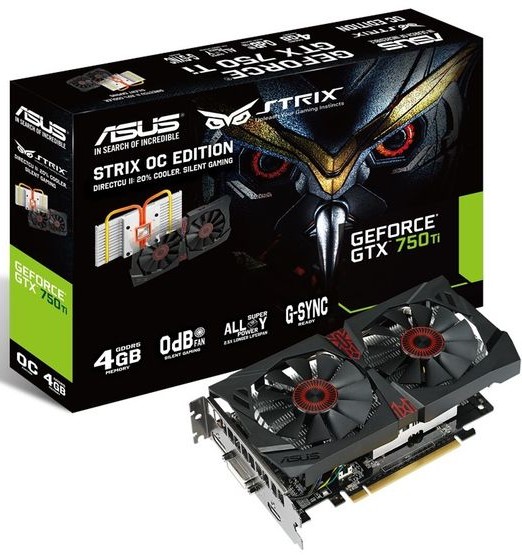
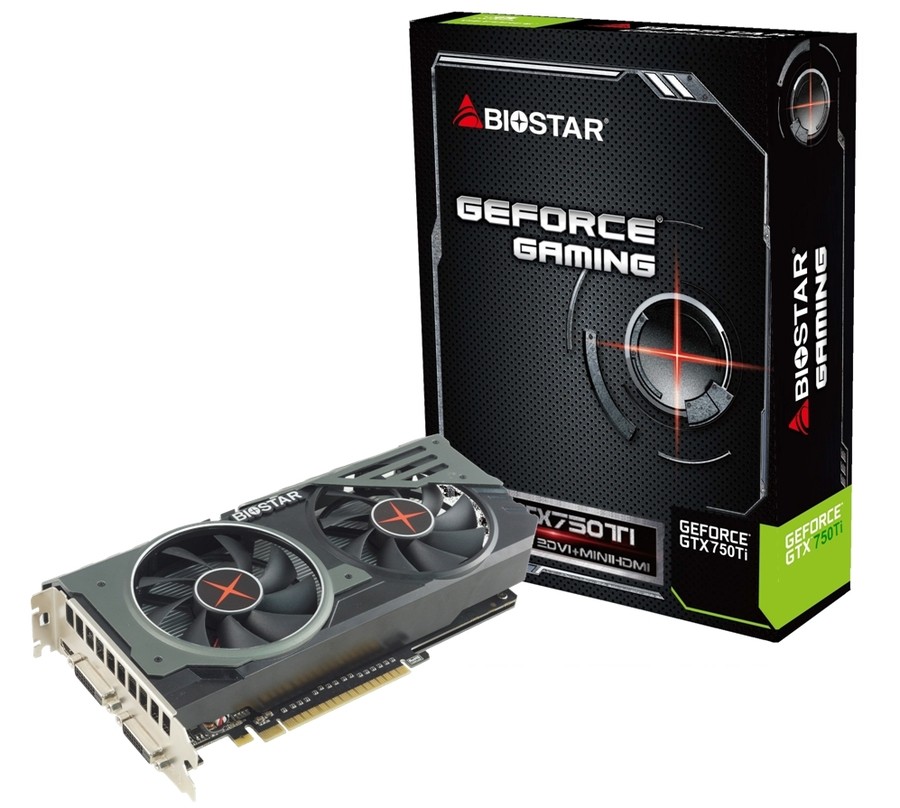
TechPowerUp today released the latest version of TechPowerUp GPU-Z, the popular graphics subsystem information and diagnostics utility. Version 2.11.0 introduces support for NVIDIA GeForce RTX 20-series "Turing" graphics cards, including the RTX 2080 Ti, RTX 2080, and RTX 2070. Support is also added for a few exotic OEM variants we discovered over the months, including GTX 750 Ti (GM107-A), GTX 1050 Ti Mobile 4 GB, Quadro P1000, Tesla P100 DGXS, GeForce 9200. From the AMD stable, we add support for "Vega 20," "Fenghuang" semi-custom SoC for Zhongshan Subor, Ryzen 5 Pro 2500U, 5 Pro 2400G, 3 Pro 2200G, 3 Pro 2300U, 3 2200GE, Athlon 200GE, and Embedded V1807B. Intel UHD 610, UHD P630 (Xeon), Coffee Lake GT3e (i5-8259U), are now supported.

Among the new features are system RAM usage sensors, temperature monitoring offsets for AMD Ryzen Threadripper 2000 series processors, and the ability to identify USB-C display output, GDDR6 memory standard, and 16 Gbit density memory chips. Several under-the-hood improvements were made, including WDDM-based memory monitoring for AMD GPUs, replacing ADL sensors that tend to be buggy. GPU-Z also cleans up QueryExternal files from your Temp folder. Grab GPU-Z from the link below.
DOWNLOAD: TechPowerUp GPU-Z v2.11.0

The change-log follows.

ASUS Announces GeForce GTX 750 Ti Strix 4GB

In a bid to woo those who choose graphics cards by memory amounts (and cars with engine-displacement), ASUS rolled out a 4 GB variant of its GeForce GTX 750 Ti Strix lower mid-range graphics card. Pictured below, the card is built identical to the standard 2 GB model, but with double the GDDR5 memory amount. It features out of the box clock speeds of 1124 MHz core, 1202 MHz GPU Boost, and 5.40 GHz (GDDR5-effective) memory. Based on the 28 nm GM107 silicon, the GTX 750 Ti features 640 CUDA cores based on the "Maxwell" architecture, and a 128-bit wide GDDR5 memory interface. ASUS didn't disclose pricing.

Biostar Outs GeForce GTX 750 Ti Gaming OC Graphics Card

Biostar made a comeback to graphics cards after a long sabbatical, with a new GeForce GTX 750 Ti based graphics card, the GTX 750 Ti Gaming OC. Based on a custom-design that we guess could be originally designed by either Onda or Galaxy, the card features a custom-design dual-fan cooling solution, which consists of a solid aluminium heatsink, which is ventilated by a pair of 80 mm spinners. The card offers factory overclocked speeds of 1059 MHz core, 1137 MHz GPU Boost, and an untouched 5.40 GHz memory, compared to reference speeds of 1020/1085 MHz. Display outputs include two dual-link DVI, and a mini-HDMI. The card features 2 GB of GDDR5 memory, across its 128-bit wide memory interface. Based on the 28 nm GM107 silicon, the GTX 750 Ti features 640 CUDA cores based on the "Maxwell" architecture.

Even More GeForce GTX 980 and GM204 Specs Tumble Out

Ahead of its launch later this week, even more details of NVIDIA's upcoming GeForce GTX 980, and the 28 nm "GM204" silicon it's based on, tumbled out. To begin with, the GM204 silicon is confirmed to be built on the 28 nm silicon fab process. The chip bigger than that of the GK104, with a die area of 398 mm², yet smaller than the GK110, which measures 581 mm². Its transistor count is 5.2 billion, about 2 billion more than the GK104.

The component hierarchy of GM204 is similar to that of the GM107 silicon, on which the GTX 750 Ti is based. The GPU features a 256-bit wide GDDR5 memory interface, and PCI-Express 3.0 x16 bus. The GigaThread Engine dispatches workload between four graphics processing clusters (GPCs), the basic subunit. Each GPC has a common raster engine shared between four streaming multiprocessors Maxwell (SMMs), which each hold 128 CUDA cores. The total CUDA core count is hence 2,048. The L2 cache has been quadrupled over GK104. The chip features 2 MB of it, compared to 512 KB on its predecessor. The GM204 features 64 ROPs, double that of the GK104, and should hence come with a strong geometry processing muscle. The chip features a revolutionary new 3-bit delta color compression technology that makes the most of the limited memory bus width of this chip.

AMD "Tonga" GPU Arrives This August

In a bid to counter NVIDIA's bestselling GeForce GTX 760, AMD is preparing a new 28 nm GPU, codenamed "Tonga," as detailed in our older article on the chip. At the time of its writing, we had two theories on what "Tonga" could be, one held that it could be a counter to the GM107, and the other, that's is a step above "Curacao," in a bid to counter the GTX 760. We're now learning that AMD could launch the first graphics cards based on this chip, some time in August. The chip will replace the ailing "Tahiti Pro" silicon, from which is carved out the Radeon R9 280. While the R9 280 offers performance competitive to the GTX 760, it loses out big time on power consumption and heat. The cheaper R9 270X, on the other hand, offers lower performance, and similar power levels. "Tonga" could offer nearly as much performance, while featuring a new combination of components, that help AMD lower not just power draw, but also overall costs.

The 28 nm "Tonga" silicon is expected to feature 2,048 GCN2 stream processors, 128 TMUs, 32 ROPs, and a 256-bit wide GDDR5 memory interface. You'll notice that its memory interface is narrower than that of the R9 280, but performance is made up for with a higher stream processor count, and probably higher clock speeds, too. The card could come in memory capacities of 2 GB, with some manufacturers innovating 4 GB variants. There's no word on what the company could end up naming the first cards running this chip.

AMD Readies 28 nm "Tonga" to Take on GM107

NVIDIA's energy-efficiency leap achieved on existing 28 nanometer process, using the "Maxwell" based GM107, appears to have rattled AMD. The company is reportedly attempting a super-efficient, 28 nm, mid-range chip of its own, codenamed "Tonga." The chip could power graphics cards that compete with the GeForce GTX 750 Ti and GTX 750. The chip is likely to be based on Graphics CoreNext 2.0 micro-architecture, the same one that drives "Hawaii," which means AMD isn't counting on the micro-architecture for efficiency gains. It could feature an evolution of PowerTune, which works closer to the metal than its existing implementation on "Hawaii." Other features could include Mantle, TrueAudio, and perhaps even XDMA CrossFire (no cables needed). The chip could be wired to up to 2 GB of memory.

Another equally plausible theory doing rounds is that "Tonga" could be a replacement to "Tahiti Pro," designed to compete with the GK104 at much lower power footprint (than "Tahiti"), so AMD could more effectively compete with the GeForce GTX 760. The chip could be similar in feature-set to "Tahiti," with a narrower memory bus (256-bit wide), but higher clock speeds to make up for it. If this theory holds true, then "Tonga" could disrupt both Tahiti Pro and "Curacao XT." Curacao XT (R9 270X) is designed to offer a value-conscious alternative to the $250 GTX 760. The R9 280 is competitive in performance, but takes a beating on the energy-efficiency front, and is also costlier to manufacture, due to the higher transistor count and four additional memory chips. We could hear more at Computex 2014.

GIGABYTE Readies Black Edition GeForce GTX 750 Ti Card

GIGABYTE Technology will soon be releasing a new GeForce GTX 750 Ti card, a model codenamed GV-N75TWF2BK-2GI which bears the 'Black Edition' tag, meaning it has underwent a 168-hour server level stress test to ensure top-notch durability. A certificate of validation will be bundled to show the card survived testing.

Pictured below, the Black Edition GTX 750 Ti comes equipped with a WindForce 2X cooler and has 640 CUDA Cores, a 128-bit memory interface, 2 GB of GDDR5 VRAM set to 5400 MHz, dual DVI and dual (gold-plated) HDMI outputs, and a GM107 GPU with Base/Boost clocks of 1033/1111 MHz for the base model and 1163/1242 MHz for the OC edition. No word on prices yet.

EVGA Announces GeForce GTX 750 FTW 2GB

EVGA announced an Amazon-exclusive 2 GB variant of its GeForce GTX 750 FTW graphics card (model: 02G-P4-2758-KR). Built in an identical board design to the original GTX 750 FTW, with the company's ACX cooling solution, the card offers factory-overclocked speeds of 1229 MHz core, 1320 MHz GPU Boost, and 5012 MHz (GDDR5-effective) memory, and features 2 GB of it across the chip's 128-bit wide memory interface. The cooling solution is designed to deal with much bigger chips, and should keep the GTX 750 quiet and comfy, even at its maker-given speeds. Based on the 28 nm GM107 silicon, the GTX 750 packs 512 CUDA cores, and is based on NVIDIA's new "Maxwell" GPU architecture. The card is priced at US $149.99.

NVIDIA GeForce GTX 860M Detailed

NVIDIA slipped out the first mobile GPU based on its GM107 silicon, the GeForce GTX 860M, which was spotted on the forumscape. The GTX 860M is configured identically to the desktop GTX 750 Ti, featuring the chip's full complement of 640 CUDA cores, 40 TMUs, 16 ROPs, and a 128-bit wide GDDR5 memory interface, holding 2 GB of memory. The core is clocked at 540 MHz, and the memory at 5.00 GHz (GDDR5 effective).

The mobile MXM card was put through a battery of synthetic tests, in which it was found to be twice as fast as its predecessor, the GTX 660M. In 3DMark 11 (performance preset), it scored P5339, compared to the P2563 points scored by the GTX 660M. In 3DMark 11 (extreme preset), the story is similar, with the GTX 860M scoring X1662, compared to the X774 scored by the GTX 660M.

GM107 Features 128 CUDA Cores Per Streaming Multiprocessor

NVIDIA's upcoming GM107 GPU, the first to be based on its next-generation "Maxwell" GPU architecture, reportedly features a different arrangement of CUDA cores and streaming multiprocessors to those typically associated with "Kepler," although the component hierarchy is similar. The chip reportedly features five streaming multiprocessors, highly integrated computation subunits of the GPU. NVIDIA is referring to these parts as "streaming multiprocessor (Maxwell)," or SMMs.

Further, each streaming multiprocessor features 128 CUDA cores, and not the 192 CUDA cores found in SMX units of "Kepler" GPUs. If true, GM107 features 640 CUDA cores, all of which will be enabled on the GeForce GTX 750 Ti. If NVIDIA is carving out the GTX 750 by disabling one of those streaming multiprocessors, its CUDA core count works out to be 512. NVIDIA will apparently build two GPUs on the existing 28 nm process, the GM107, and the smaller GM108; and three higher performing chips on the next-generation 20 nm process, the GM206, the GM204, and the GM200. The three, as you might have figured out, succeed the GK106, GK104, and GK110, respectively.

GTX 750 Taken Apart, Sips Power from a Single 6-pin Connector

Here are the first pictures of a partner-branded GeForce GTX 750 graphics card taken apart. It reveals a couple of things - to begin with, the GM107 silicon will bring about some genuine performance per Watt improvements, despite being based on the existing 28 nm silicon fab process, and second, that cards based on the chip will be extremely cheap to build, giving NVIDIA a good chance to strengthen its position in the sub-$200 market segment. This particular card is cooled by a simple fan-heatsink that's essentially a chunk of metal with a fan latched on to it. The card relies on a simple 2+1 phase VRM, which draws power from a single 6-pin PCIe power connector. NVIDIA is expected to launch the GTX 750 and GTX 750 Ti a little later this month.

AIC Branded GeForce GTX 750 Ti and GTX 750 Pictured, Clock Speeds Surface

Here are the firs pictures of AIC partner branded GeForce GTX 750 Ti and GTX 750 graphics cards. From the looks of the board design the first two AIC partners that come to mind are Palit and Galaxy. Specifications of the GM107 silicon, on which the two are based, is detailed in our older article with a die-shot. What's new here, however, is that CUDA core counts and clock speeds aren't the only two specifications that separate the GTX 750 Ti from the GTX 750; it's also the standard memory amount. The former will ship with 2 GB of it, while the latter just 1 GB.

British tech publication UK Gaming Computers got their hands on the two cards, and took a peek under the hood using GPU-Z 0.7.6 (which supports the two). It confirms specifications from the older article, and also reveals clock speeds. The GTX 750 Ti features 1085 MHz core, 1163 MHz GPU Boost, and 5.50 GHz (GDDR5-effective) memory, which churns out 88 GB/s of memory bandwidth. The GTX 750, on the other hand, features the same GPU clock speeds, but slightly slower memory, at 5.10 GHz, at which the memory bandwidth is 81 GB/s. The site also put the two through a quick 3DMark 11 run (performance preset). The GTX 750 Ti scored P5963 points, and the GTX 750 scored P5250 points. Since the two are custom design cards, we're not sure if the clock speeds will stick. For all we know, the two could be factory-overclocked. Impressive performance nonetheless.

NVIDIA GM107 "Maxwell" Silicon Pictured

Here is the first picture of a couple of NVIDIA GM107 silicons in a tray, ahead of graphics card assembly. The packages appear to be as big as those of the GK106 from the previous generation, however, the die itself is estimated to be smaller, at roughly 156 mm², compared to the 221 mm² die of the GK106, and the 118 mm² of the GK107. The best part? All three chips are built on the same 28 nm silicon fab process. So what makes the GM107 die smaller than that of the GK106 despite having a similar feature-set? Narrower memory bus. The GM107 is said to feature a 128-bit wide GDDR5 memory interface, in comparison to the 192-bit wide interface of the GK106.

Apart from the 128-bit wide GDDR5 memory interface, the GM107 is said to feature a total of 960 CUDA cores, 80 TMUs, and 16 ROPs. The CUDA core count is identical to that of the GK106. The GM107 is built on NVIDIA's next-generation "Maxwell" GPU architecture. It will form the foundation of two SKUs, the GeForce GTX 750 Ti, and the GeForce GTX 750. The former features the full complement of 960 CUDA cores; while the latter is slightly cut down, and features just 768. The TDP of the GTX 750 Ti is approximated to be around 75 Watt. If true, the GTX 750 duo will set new standards on the performance-per-Watt metrics. NVIDIA is expected to launch both, later this month.
Return to Keyword Browsing
Apr 19th, 2024 18:47 EDT change timezone

New Forum Posts

Popular Reviews

Controversial News Posts