News Posts matching #Tonga

Return to Keyword Browsing

AMD Teases Polaris 10 and Polaris 11 ASIC Images

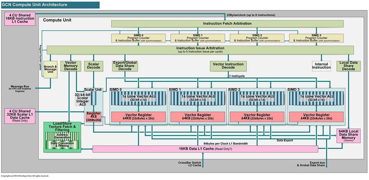
AMD posted a new webpage for its upcoming "Polaris" GPU architecture, outlining its various innovations - 4th gen. Graphics CoreNext, 4K H.265 60 Hz game-streaming, next-generation display engine with support for DisplayPort 1.3 and HDMI 2.0, XConnect Technology, and the foundation of GPUOpen. In this page, the company inadvertently leaked pictures of its upcoming Polaris 10 "Ellesmere" and Polaris 11 "Baffin" ASICs.

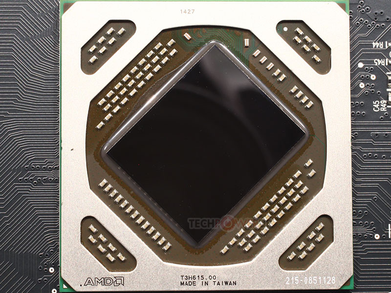
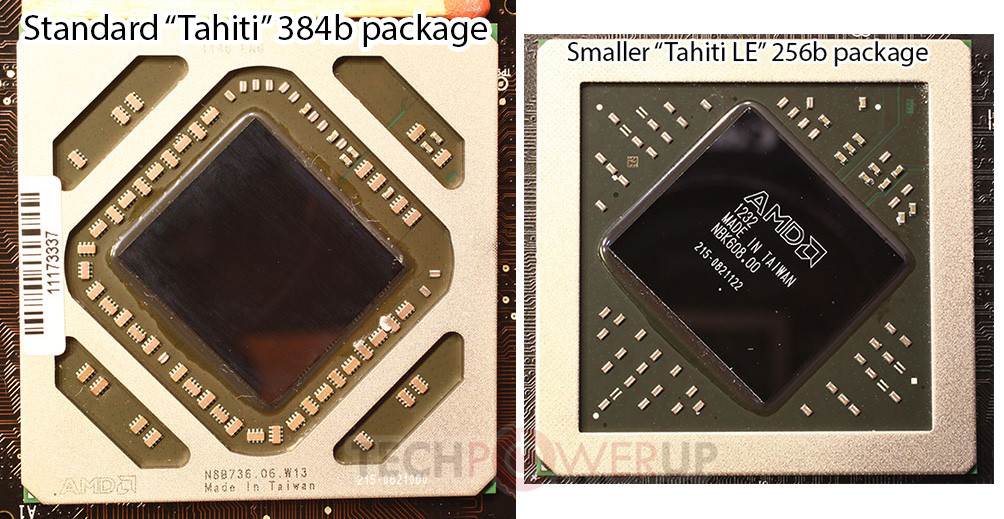
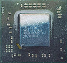
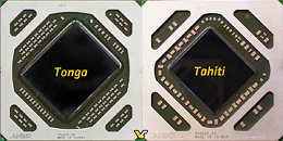
The mast image of the page has a faded 3-quarter shot of a "small" GPU with a die that's almost 30% of the package area. This hints at Polaris 11 "Baffin." This chip is rumored to feature a 128-bit GDDR5/GDDR5X memory interface, and so its pin-count, and conversely, package-size is less. Then in its "4th gen GCN" heading image, AMD showed a picture of a bigger GPU. At first glance, you could assume that it's either "Tonga XT" or "Tahiti" looking at its support brace, but VideoCardz observed that the on-package electrical components in this image are arranged nothing like on the "Tonga" or "Tahiti." This could very well be Polaris 10 "Ellesmere."

AMD Outs "Bristol Ridge" APU Performance Numbers

Although AMD's upcoming socket AM4 heralds new lines of processors and APUs based on the company's next-generation "Zen" CPU micro-architecture, some of the first APUs will continue to be based the current "Excavator" architecture. The "Bristol Ridge" is one such chip. It made its mobile debut as the 7th generation A-Series and FX-Series mobile APUs, and is en route to the desktop platform, in the AM4 package. What sets the AM4 package apart from the FM2+ package, and in turn "Bristol Ridge" from "Carrizo" is that the platform integrates even the southbridge (FCH) into the APU die. This could explain the 1,331-pin count of the AM4 socket.

The "Bristol Ridge" silicon is likely built on the existing 28 nm process. That's not the only thing "current-gen" about this chip. Its CPU component consists of two "Excavator" modules that make up four CPU cores, with 4 MB total cache; and its integrated GPU will likely be based on the Graphics CoreNext 1.2 "Volcanic Islands" architecture, the same one which drives the "Tonga" and "Fiji" discrete GPUs. The integrated memory controller supports dual-channel DDR4 memory. In its performance benchmarks, an AM4 APU based on the "Bristol Ridge" silicon was pitted against older 6th generation APUs, in which it was found to be as much as 23 percent faster.

AMD Announces the Radeon R9 380X Graphics Card

AMD announced the Radeon R9 380X graphics card. Positioned between the Radeon R9 380 and the R9 390, this card starts at US $229, and takes advantage of a huge gap in NVIDIA's lineup, between the GeForce GTX 960 ($190) and the GTX 970 ($319). Based on the 28 nm "Antigua" ("Tonga") silicon, this SKU features the full complement of the chip's 32 Graphics CoreNext (GCN) compute units, amounting to 2,048 stream processors. It also features 128 TMUs, 32 ROPs, and a 256-bit wide GDDR5 memory interface, holding 4 GB of memory. The core is clocked at 970 MHz, and the memory at 5.70 GHz (GDDR5-effective), amounting to a memory bandwidth of 182 GB/s.

Three AIB Branded Radeon R9 380X Graphics Cards Pictured

Here are the first pictures of three AIB-branded Radeon R9 380X graphics cards, including one each from ASUS, XFX, and GIGABYTE. The ASUS branded Radeon R9 380X graphics card, the R9 380X STRIX, features the company's dual-slot, dual-fan DirectCU II cooling solution. ASUS is also giving it a slick back-plate, and offering it in two variants based on factory-overclock (or lack of it).

The XFX branded R9 380X features a similar product size to the ASUS card, featuring a moderately long PCB, and a dual-slot, dual-fan "Double Dissipation" cooler. XFX will sell variants of this card in reference and factory-overclocked speeds. Lastly, there's GIGABYTE. Like the others, this card features a medium-size PCB, with the company's dual-slot WindForce 2X cooling solution. Based on the 28 nm "Tonga" aka "Antigua" silicon, the R9 380X reportedly features 2,048 GCN 1.2 stream processors, 128 TMUs, 32 ROPs, and a 256-bit wide GDDR5 memory interface, holding 4 GB of memory. It's expected to launch later this week.
Souces: VideoCardz, HardwareInfo, WCCFTech

AMD Radeon R9 380X to Formally Launch This Month

Although the first Radeon R9 380X graphics cards began appearing in the press way back as mid-September, it's only in mid-November, the 15th to be precise, that AMD plans to formally launch this new performance-segment SKU. Priced at US $249, the R9 380X will be positioned between the $300+ R9 390/GTX 970; and the $200-ish R9 380, capitalizing on a gaping hole in NVIDIA's product stack, between the GTX 960 and the GTX 970.

The R9 380X will be based on the same exact silicon as the R9 380, and the same exact compact package, with pins for 256-bit wide GDDR5 memory interface; and not the 384-bit interface that the "Tonga" aka "Antigua" silicon physically supports. All 32 Graphics CoreNext compute units (CUs) will be enabled, yielding 2,048 stream processors. The chip will also feature 128 TMUs and 32 ROPs. The core could be clocked as high as 1100 MHz, and memory at 6.00 GHz (GDDR5-effective). 4 GB will be the standard memory amount. There won't be a reference design, and AMD AIB partners will be ready with custom-design products from day-one.

AMD "Fiji" GPU Die-shot Revealed by Chipworks

VLSI technical publication Chipworks posted the first clear die-shot of AMD's "Fiji" silicon, revealing intricate details of the most technically advanced GPU. What makes Fiji the most advanced graphics chip is its silicon interposer and stacked HBM chips making up a multi-chip module. It's the die in the center of all that, which went under Chipworks' microscope.

The die-shot reveals a component layout that's more or less an upscale of "Tonga." Some of the components, such as the front-end appear to be entirely identical to "Tahiti" or "Tonga." The shot reveals the 64 GCN compute units arranged in four rows, on either side of the central portion with the dispatch and primitive setup pipelines. The pad-area of the on-die memory controllers appear to be less than the large memory I/O pads that made up the 384-bit interface of "Tahiti." The first picture below is the die-shot of "Fiji," followed by a color-coded die-shot of "Tahiti."

AMD Readies Radeon R9 380X, XFX Ready with Card

AMD is readying a new SKU to take advantage of the vast pricing gap between the GeForce GTX 960 and GTX 970, and to bolster its sub-$300 lineup, with the Radeon R9 380X. This SKU will be based on the 28 nm "Tonga" silicon, which implements the latest Graphics CoreNext 1.2 architecture. The R9 380X could max out the specifications of the "Tonga" silicon, offering 2,048 stream processors spread across 32 compute units, 128 TMUs, 32 ROPs, and a 384-bit wide GDDR5 memory interface, holding either 3 GB or 6 GB of memory.

Another equally plausible theory pins the R9 380X as a chip with 2,048 stream processors, but the same 256-bit GDDR5 memory interface of the R9 380, with 4 GB of memory, letting AMD keep the costs low. XFX appears to be ready with a "Double Dissipation" card based on the R9 380X. The card's new-generation Double Dissipation cooler features an aluminium fin-stack heatsink with four 8 mm thick nickel-plated copper heat pipes, and a pair of 100 mm spinners, which are easily detachable, letting you clean the heatsink underneath. Mass-production of the R9 380X is reportedly underway, so a launch is to be expected rather soon.

AMD Didn't Get the R9 Fury X Wrong, but NVIDIA Got its GTX 980 Ti Right

This has been a roller-coaster month for high-end PC graphics. The timing of NVIDIA's GeForce GTX 980 Ti launch had us giving finishing touches to its review with our bags to Taipei still not packed. When it launched, the GTX 980 Ti set AMD a performance target and a price target. Then began a 3-week wait for AMD to launch its Radeon R9 Fury X graphics card. The dance is done, the dust has settled, and we know who has won - nobody. AMD didn't get the R9 Fury X wrong, but NVIDIA got its GTX 980 Ti right. At best, this stalemate yielded a 4K-capable single-GPU graphics option from each brand at $650. You already had those in the form of the $650-ish Radeon R9 295X2, or a pair GTX 970 cards. Those with no plans of a 4K display already had great options in the form of the GTX 970, and price-cut R9 290X.

The Radeon R9 290 series launch from Fall-2013 stirred up the high-end graphics market in a big way. The $399 R9 290 made NVIDIA look comically evil for asking $999 for the card it beat, the GTX TITAN; while the R9 290X remained the fastest single-GPU option, at $550, till NVIDIA launched the $699 GTX 780 Ti, to get people back to paying through their noses for the extra performance. Then there were two UFO sightings in the form of the GTX TITAN Black, and the GTX TITAN-Z, which made no tangible contributions to consumer choice. Sure, they gave you full double-precision floating point (DPFP) performance, but DPFP is of no use to gamers. So what could have been the calculation at AMD and NVIDIA as June 2015 approached? Here's a theory.
Image credit: Mahspoonis2big, Reddit

AMD Also Announces Radeon R9 380 Performance-segment Graphics

In addition to the Radeon R7 300 series, AMD announced the Radeon R9 380 performance-segment graphics card. Available in 2 GB and 4 GB variants, with the 2 GB variant priced at $199, to compete with NVIDIA's GeForce GTX 960, and the 4 GB variant about $50 costlier, the card can play any of today's games at 1080p, with eye-candy maxed out, but can also play them at 1440p, with reasonably high settings.

Based on the 28 nm "Tonga" silicon, the R9 380 packs 1,792 stream processors based on the latest GCN 1.2 architecture, with 112 TMUs, 32 ROPs, and up to 4 GB of memory across a 256-bit wide memory interface. Its core is clocked at 970 MHz, with the memory at 5.70 GHz (GDDR5 effective), churning up 184 GB/s of memory bandwidth. The card's typical power draw is rated at 190W, it draws power from a pair of 6-pin PCIe power connectors.

AMD Radeon Graphics Roadmap for 2015 Leaked

It looks like AMD's desktop discrete GPU lineup for 2015 will see a mix of rebrands, re-codename, and one big new chip, all making up the new Radeon R7 300 and R9 300 series. Cards based in this lineup should begin rolling out this month. Leaks from OEMs such as this one, suggest that the first of these should begin rolling out as early as June 16.

The spread is pretty cut and dry. "Hawaii," the chip driving the R9 290 series, will not only get a new codename as "Grenada," but also a seamless rebrand to the R9 390 series, with Grenada Pro making up the R9 390, and Grenada XT making up the R9 390X. One possibility could be AMD taking advantage of low 4 Gbit GDDR5 chip prices to cram 8 GB of standard memory amount, across Grenada's 512-bit wide memory interface. The R9 390X will compete with the GeForce GTX 970, while the R9 390 will offer an option in the vast price and performance gorge between the GTX 960 and GTX 970.

AMD Radeon R9 380 Launched by PC OEM

Earlier this day, HP announced its newest line of desktop PCs, one of which comes with a curious-sounding Radeon R9 380 graphics card. HP's product pages for its new desktops aren't active, yet, leaving us to only speculate on what the R9 380 could be. One theory making rounds says that the R9 380 could either be a re-branded R9 285, or be based on its "Tonga" silicon, which physically features 2,048 stream processors based on Graphics CoreNext (GCN) 1.2 architecture, and a 384-bit wide GDDR5 memory interface. Another theory states that the R9 380 could be an OEM-only re-brand of the R9 280 or R9 280X, based on the 3+ year old "Tahiti" silicon.

The former theory sounds more plausible, because re-branding a "Tahiti" based product would be suicidal for AMD. Although based on GCN, "Tahiti" lacks a lot of architecture features introduced with "Hawaii" and "Tonga." AMD practically stopped optimizing games for "Tahiti," and some of its new features, such as FreeSync and XDMA CrossFire, can't be implemented on it. "Tonga," on the other hand, supports both these features, and one can create an SKU with all its 2,048 stream processors, and its full 384-bit GDDR5 memory interface unlocked. If the R9 380 is indeed an OEM-only product, then it's likely that the company's retail-channel products could be branded in the succeeding R9 400 series. GPU makers tend to re-brand and bump their SKUs by a series for OEMs to peddle in their "new" products at short notice.

AMD Cuts Prices of Radeon R9 285

As the Spring PC upgrade season heats up, AMD decided to woo mainstream gamers away from NVIDIA's GeForce GTX 960, by working with retailers in the EU to introduce price-cuts on its Radeon R9 285 graphics card. The card can now be had for under 180€ (incl taxes). The GTX 960, in comparison, starts at 192€ (incl taxes). The R9 285 offers higher performance than the GTX 960. It is, however, let down by higher power consumption and noise figures. Based on the 28 nm "Tonga" silicon, the R9 285 offers 1,792 stream processors based on AMD's Graphics CoreNext 1.2 architecture, 112 TMUs, 32 ROPs, and a 256-bit wide memory interface, holding 2 GB of memory.

AMD R9 390 Series To Launch Alongside Computex 2015

AMD is preparing to time the launch of its next-generation Radeon R9 300 series with that of Computex 2015, in early June. The company had earlier planned to launch some products that are essentially price-adjusted rebrands of existing ones, such as the R9 380 series (being rebrands of R9 290 series on a slightly improved silicon), and the R9 370 series (being based on the "Tonga" silicon); but has decided to launch the two along with its flagship R9 390 series, based on a brand new silicon, around the same time. AMD's answer to the GTX TITAN-X from NVIDIA, the R9 390X will feature around 4,096 stream processors based on the Graphics CoreNext 1.3 architecture, and will implement an HBM (high-bandwidth memory) interface, with bandwidths in excess of 600 GB/s.

AMD to Launch New GPUs and APUs Only After March: CEO

In its an investor conference-call following its Q4-2014 and FY-2014 results, AMD stated that it will release new GPU and APU products starting Q2-2015, or only after March. "Going into the second quarter and the second half of the year with our new product launches, I think we feel very good about where we are positioned there," said Lisa Su, chief executive officer.

Q2-2015 will start off with the company's "Carrizo" line of all-in-one and notebook APUs. These chips will integrate the company's new "Excavator" CPU cores, with an integrated graphics core based on Graphics CoreNext 1.2 architecture (the same one AMD built its "Tonga" GPU on). Around the same time, AMD will launch new Opteron "Seattle" enterprise CPUs, which integrate up to eight ARM Cortex A-57 64-bit cores, targeting the ultra-dense server market. In Q2-2015, AMD will launch its latest Radeon Rx 300 series graphics processors. Its performance-segment part, the R9 380, will feature 4,096 GCN 1.2 cores, double that of its predecessor, and 4 GB of stacked HBM (high-bandwidth memory). Its mid-range chip, codenamed "Trinidad" will succeed "Curacao," and offer performance competitive to the $200-ish price-point.

EK Tonga Pro Full-Cover WaterBlock Starts Shipping

EK Water Blocks, Ljubljana based premium computer liquid cooling gear manufacturer, is proud to introduce a new Full-Cover water block for reference design AMD Radeon R9 285 series graphics cards, powered by Tonga Pro GPU.

EK-FC R9-285 is a high-performance Full-Cover water block which directly cools the GPU, RAM as well as VRM (voltage regulation module) as water flows directly over these critical areas thus allowing the graphics card and it's VRM to remain stable under high overclocks.

AMD "Tonga" Silicon Features 384-bit Wide Memory Interface

In what could explain the rather large die-size and transistor-count of AMD's "Tonga" silicon, compared to "Tahiti," it turns out that the silicon features a 384-bit wide GDDR5 memory interface, and not the previously thought of 256-bit wide one. The die is placed on a package with pins for just 256-bit, on the Radeon R9 285, but it can be placed on a bigger package, with more pins, to wire out the full width of the memory bus, in future SKUs. This isn't the first time AMD has done something like this. Its "Tahiti LE" chip was essentially a "Tahiti" die placed on a smaller package with pins for just a 256-bit wide memory bus, on the oddball Radeon HD 7870 XT.

What this means is that AMD's next performance-segment graphics card based on the "Tonga" silicon, could feature 50% more memory bandwidth than the R9 285. The stream processor count is still 2,048, but these are more advanced Graphics CoreNext 1.2 stream processors, compared to first-generation ones on "Tahiti," offering more performance per Watt. The TMU count remains 128, although there's no clarity on the ROP count. Estimates are split between 32 and 48. The R9 285 has 32, and so does "Tahiti."

AMD Readies Radeon R9 390X to Take on GeForce GTX 980

It turns out that the big OEM design win liquid cooling solutions maker Asetek was bragging about, is the Radeon R9 390X, and the "undisclosed OEM" AMD. Pictures of a cooler shroud is doing rounds on Chinese tech forums, which reveals something that's similar in design to the Radeon R9 295X2, only designed for single-GPU. The shroud has its fan intake pushed to where it normally is for single-GPU cards; with cutouts for the PCIe power connectors, and a central one, through which liquid cooling tubes pass through.

One can also take a peek at the base-plate of the cooler, which will cool the VRM and memory under the fan's air-flow. The cooler design reveals that AMD wants its reference-design cards to sound quieter "at any cost," even if it means liquid cooling solutions that can be messy with multi-card CrossFire setups, and in systems that already use liquid-cooling for the CPU; and leave it to AIB partners to come up with air-cooled cards, with meatier heatsinks. Other specs of the R9 390X are unknown, as is launch date. It could be based on a member of the "Pirate Islands" family of GPUs, of which the new "Tonga" GPU driving the R9 285 is a part of. A possible codename of AMD's big chip from this family is "Fiji."

XFX Rolls Out its Radeon R9 285 Double Dissipation Graphics Card

XFX joined the Radeon R9 285 launch party with its compact R9 285 Double Dissipation graphics card. Built on an black, custom-design, matte-finish PCB, XFX' card features a lightweight version of its twin-fan cooling solution, which has been featured on its older performance-segment cards, such as the R9 270X. The cooler features a dense aluminium fin stack, to which heat is fed by four 6 mm thick copper heat pipes, which is then ventilated by a pair of 80 mm spinners. The card sticks to AMD reference clock speeds of 918 MHz core, and 5.50 GHz (GDDR5-effective) memory. Based on the 28 nm "Tonga" silicon, the R9 285 features 1,792 Graphics CoreNext 1.2 stream processors, 112 TMUs, 32 ROPs, and a 256-bit wide GDDR5 memory interface, holding 2 GB of memory on this card. Expect it to be priced at US $249.

ASUS Announces the Radeon R9 285 Strix Graphics Card

ASUS announced the Radeon R9 285 Strix graphics card, based on AMD's latest 28 nm "Tonga" silicon. The card utilizes ASUS' latest Strix cooling solution, which stays silent until a thermal threshold is reached, only beyond which, its fans begin to spool up. Barring its new cooler shroud design and fan-speed management, the Strix cooling solution bears strong resemblance to the company's DirectCU II cooling solution. ASUS is shipping the card with a factory-overclock. Based on the 28 nm "Tonga" silicon, the R9 285 from AMD features 1,792 stream processors, 112 TMUs, 32 ROPs, and a 256-bit wide memory interface, which holds 2 GB of memory on this card.

HIS Announces its Radeon R9 285 IceQ X2 Graphics Card

HIS rolled out is IceQ X2 implementation of AMD's newest Radeon R9 285 graphics card. Available in reference clock (918 MHz core, 5.50 GHz memory), and OC variants (928 MHz core), HIS' cards sport a lightweight variant of the IceQ X2 cooler which was previously implement on the company's R9 270X graphics cards, taking advantage of the lower thermal figures of the R9 285. It appears to be based on a compact non-reference design PCB. The cooler features a dense aluminium fin-stack, cooled by a pair of 80 mm fans. Based on the 28 nm "Tonga" silicon, the R9 285 from AMD features 1,792 stream processors, 112 TMUs, 32 ROPs, and a 256-bit wide memory interface, which holds 2 GB of memory on this card.

MSI Announces its Radeon R9 285 Gaming OC Graphics Card

MSI announced its first Radeon R9 285 graphics card, built in its successful Gaming Series, featuring the company's TwinFrozr IV compact cooling solution, which the company deployed on several of its performance-segment graphics cards, such as the R9 280, the GTX 770, etc. The card also features a factory overclock of 1000 MHz, compared to reference clock speeds of 918 MHz core and 5.50 GHz (GDDR5-effective) memory. Based on the 28 nm "Tonga" silicon, the R9 285 from AMD features 1,792 stream processors, 112 TMUs, 32 ROPs, and a 256-bit wide memory interface, which holds 2 GB of memory on this card.

AMD Announces the Radeon R9 285 Performance Graphics Processor

AMD announced its most important GPU for the season, the Radeon R9 285. The chip is designed to compete with the GeForce GTX 760 from NVIDIA at not just performance, but also energy-efficiency, and low component costs, so AMD can price it better. Based on a brand new 28 nm silicon by the company, codenamed "Tonga," the R9 285 features 1,792 Graphics CoreNext 1.2 stream processors, 112 TMUs, 32 ROPs, and a 256-bit wide GDDR5 memory interface, holding 2 GB of memory.

AMD partners are free to come up with 4 GB variants. The card supports DirectX 12, OpenGL 4.4, and Mantle. It features new AMD innovations, such as XDMA CrossFire, TrueAudio DSP, and 4-display Eyefinity by plugging into every connector on the card (two dual-link DVI, one DisplayPort 1.2, and one HDMI 1.4a). The card draws power from a pair of 6-pin PCIe power connectors. Available now, the Radeon R9 285, from various AMD partners starts at US $249.

PowerColor Radeon R9 285 TurboDuo Detailed

Here are some of the first high-resolution pictures of the Radeon R9 285 TurboDuo graphics card by PowerColor. The card features a meaty custom-design cooling solution, with two twin-impeller fans, and a dense aluminium fin-stack heatsink. PowerColor didn't bother with a reference-clock variant of this card. It comes factory-overclocked, at 945 MHz core (918 MHz reference), and 5.50 GHz (GDDR5-effective) memory. It features 2 GB of it.

Based on the 28 nm "Tonga" silicon, the Radeon R9 285 features 1,792 Graphics CoreNext 1.1 stream processors, 112 TMUs, 32 ROPs, and a 256-bit wide GDDR5 memory interface. The card draws power from two 6-pin PCIe power connectors. Display outputs include two dual-link DVI, and one each of HDMI and DisplayPort. With a modern XDMA CrossFire interface, the card lacks CrossFire fingers. It remains to be seen just how many cards the driver allows you to run in tandem. The Radeon R9 285 from AMD will launch on the 2nd of September, 2014. Prices start at US $249.

Sapphire Radeon R9 285 ITX Compact Edition Pictured

Sapphire launched its first performance-segment "compact" graphics card to take on the likes of GeForce GTX 760 ITX cards by ASUS and MSI, even if it isn't the first AMD AIB partner to do so. Sapphire's card is based on AMD's swanky new Radeon R9 285 graphics chip, which is slated for September 2nd, 2014. Called the R9 285 ITX Compact Edition, the card is a little over 17 cm long, 11 cm tall, and 2-slot thick. It features a dense aluminium fin-stack heatsink, which is ventilated by a single 100 mm fan. The card draws power from two 6-pin PCIe connectors. A single 8-pin to two 6-pin adapter is included. Display outputs include two mini-DisplayPort 1.2, one HDMI 1.4a, and a dual-link DVI, which has analog (VGA) pins, and an adapter for that is included.

This is also likely the first/only R9 285 card to feature dual-BIOS, with a push-type BIOS toggle switch. This switch lets you select between a UEFI-ready BIOS that features a UEFI GOP driver, and a "legacy" BIOS. Both run the card at the same clock speeds - 918 MHz core, with 5.50 GHz (GDDR5-effective) memory. Sapphire is also readying an OC Edition variant of this card, which comes with a puny 10 MHz overclock (928 MHz core), and untouched memory clocks. Based on the 28 nm "Tonga" silicon, the R9 285 offers 1,792 GCN 1.1 stream processors, 112 TMUs, 32 ROPs, and a 256-bit wide memory interface, which holds 2 GB of memory on this card.

ASUS Radeon R9 285 Strix Graphics Card Pictured

Here are some of the first detailed shots of ASUS' premium custom-design Radeon R9 285 Strix graphics card, based on AMD's upcoming GPU. The card features a unique cooling solution that keeps its fans off until the GPU reaches a temperature threshold. The cooler's underlying heatsink is essentially DirectCU II, featuring a dense aluminium fin stack to which heat drawn directly from the GPU die is fed by a number of nickel-plated copper heat pipes. This particular card features a factory-overclock, and 2 GB of memory. Oh, and it comes with a back-plate. Based on the 28 nm "Tonga" silicon, the R9 285 features 1,792 Graphics CoreNext 1.1 stream processors, 112 TMUs, 32 ROPs, and a 256-bit wide GDDR5 memory interface. The card is set to launch on 2nd September, 2014. It will start at US $249.
Return to Keyword Browsing
Apr 19th, 2024 12:28 EDT change timezone

New Forum Posts

Popular Reviews

Controversial News Posts