News Posts matching #engineering sample

Return to Keyword Browsing

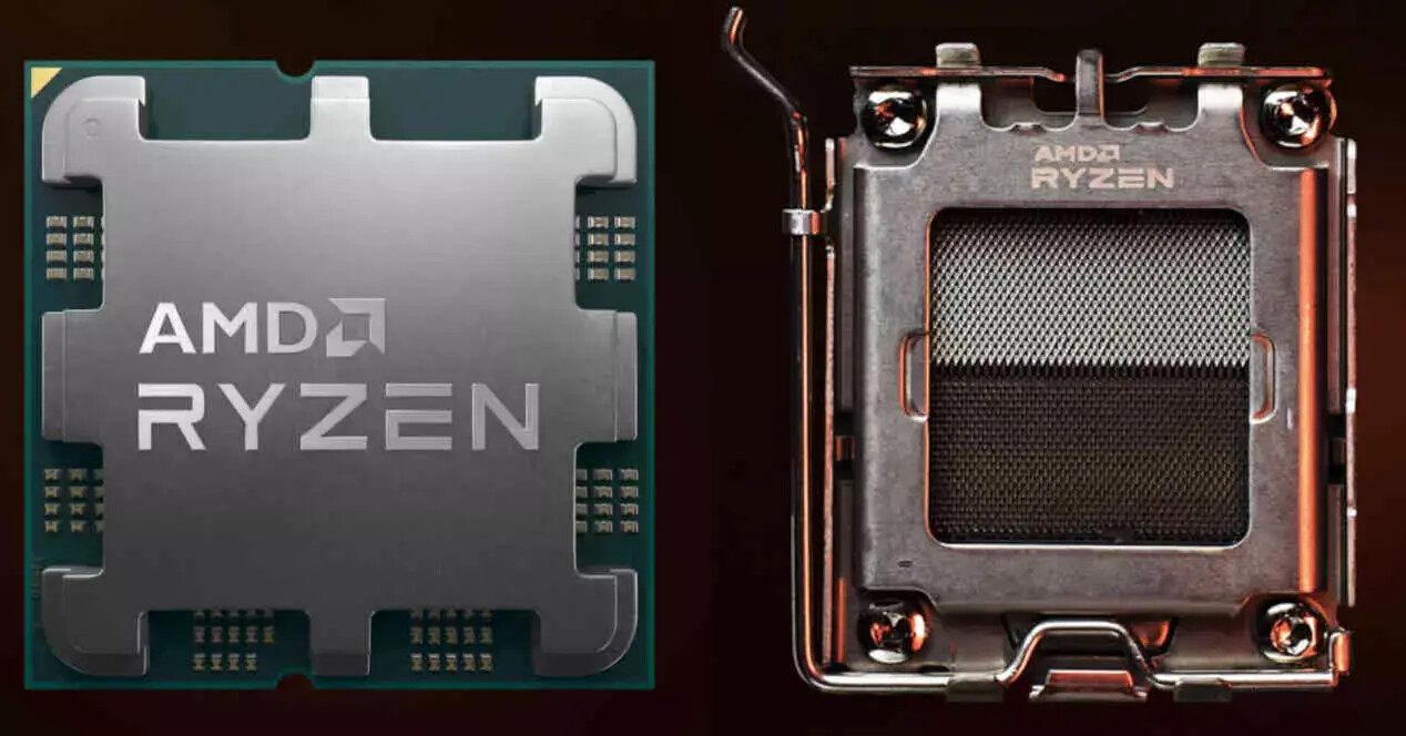
Alleged AMD Ryzen "Granite Ridge" Engineering Samples Pop Up in Shipping Manifests

Shipping manifests appear to be great sources of pre-release information—only a few hours ago, the existence of prototype AMD "Strix Point" and "Fire Range" mobile processors was highlighted by hardware sleuth harukaze5719. A related leak has appeared online fairly quickly after the discovery of laptop-oriented "Zen 5" chips. momomo_us joined in on the fun, with their exposure of speculated desktop silicon. Two brand-new AMD OPN codes have been linked to the upcoming "Granite Ridge" series of AM5 processors.

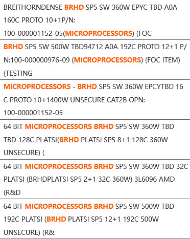
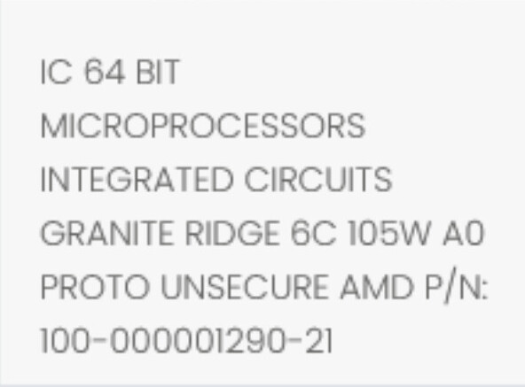
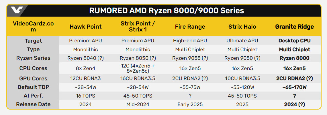
100-000001404-01 is likely an eight-core/ sixteen-thread "Zen 5" Ryzen CPU with a 170 W TDP—a stepping designation, B0, indicates engineering sample status. The other listing, 100-000001290-21, seems to be an A0-type engineering sample—leaked info suggests that this a six-core/twelve-thread (105 W TDP) next-gen mainstream desktop processor. AMD is likely nearing the finish line with its Ryzen 9000-series—a new generation of chipsets, including X870E, is reportedly in the pipeline. Additionally, VideoCardz posits that a refresh of 700-series boards could be on the cards. "Granite Range" CPUs are expected to retain the current-gen 6 nm client I/O die (cIOD), as sported by "Raphael" Ryzen 7000-series desktop processors.

AMD Ryzen 7 8700GE Engineering Sample Compared to Standard 8700G APU

Last week, AMD's Ryzen 8000GE desktop APU lineup appeared online—four lower power (TDP of 35 W) SKUs are set to join the already released 65 W TDP AM5 "Hawk Point" family. GucksTV has acquired a flagship 8000GE model, albeit in engineering sample form—a Hong Kong-based Ebay Store lists "AMD Ryzen 7 8700GE ES Tray" processors. At the time of writing only one unit remains in stock, priced at $298.99 with the option for free international delivery. The "hugohk" shop appears to specialize in supplying all sorts of Team Red engineering sample CPUs. GucksTV's German language video review pitches the Ryzen 7 8700GE engineering sample against the finalized retail release Ryzen 7 8700 APU.

AMD has not made any official release date announcements regarding the leaked Ryzen 8000GE range, but VideoCardz believes that "expectations are high that these variants will hit the market soon through system integrators." The GucksTV comparison video shows that: "On average, the single-core of 8700GE performance drops by 5%, while multi-core is 17% below 8700G. For graphics, that's a 23% average drop in performance while requiring 52% less power." The reviewer noted that his engineering sample was not allowing access to memory OC profiles, until a motherboard BIOS update was implemented (most likely via Beta firmware)—granting 6400 MT/s instead of the normal JEDEC rate of 5200 MT/s. The test platform utilized an ASRock A620I Lightning WiFi Mini-ITX mainboard—finalized Ryzen 7 8700GE APUs could be ideal candidates for usage in quiet/low temperature compact form factor systems.

Intel Lunar Lake A1 Sample CPU Boost & Cache Specs Leak Out

HXL (@9550pro) has highlighted an intriguing pinned post on the Chinese Zhihu community site—where XZiar, a self described "Central Processing Unit (CPU) expert," has shared a very fuzzy/low quality screenshot of a Windows Task Manager session. The information on display indicates that a "Genuine Intel(R) 0000 1.0 GHz" processor was in use—perhaps a very early Lunar Lake (LNL) engineering sample (ES1). XZiar confirmed the pre-release nature of the onboard chip, and teased its performance prowess: "It's good to use the craftsmanship that others have stepped on. It can run 2.8 GHz with only A1 step, and it is very smooth."

The "A1" designation implies that the leaked sample is among the first LNL processor prototypes to exit manufacturing facilities—Intel previewed its "Lunar Lake-MX" SoC package to press representatives last November. XZiar's followers have pored over the screenshot and ascertained that the leaked example sports a "8-core + 8-thread, without Hyperthreading, 4P+4LPE" configuration. Others were confused by the chip's somewhat odd on-board cache designations—L1: 836 KB, L2: 14 MB and L3: 12 MB—XZiar believes that prototype's setup "is obviously not up to par," when a replier compares the spec to an N300 series processor. It is theorized that Windows Task Manager is simply not fully capable of detecting the sample's full makeup, but XZiar reckons that 12 MB of L3 cache is the correct figure.

Intel 5th Gen Xeon Platinum 8580 CPU Details Leaked

YuuKi_AnS has brought renewed attention to an already leaked Intel "Emerald Rapids" processor—the 5th Gen Xeon Platinum 8580 CPU was identified with 60 cores and 120 threads in a previous post, but a follow up has appeared in the form of an engineering prototype (ES2-Q2SP-A0). Yuuki noted: "samples are for reference only, and the actual performance is subject to the official version." Team Blue has revealed a launch date—December 14 2023—for its 5th Gen Xeon Scalable processor lineup, so it is not surprising to see pre-release examples appear online a couple of months beforehand. This particular ES2 SKU (on A0 silicon) fields an all P-Core configuration consisting of Raptor Cove units, with a dual-chiplet design (30 cores per die). There is a significant bump up in cache sizes when compared to the current "Sapphire Rapids" generation—Wccftech outlines these allocations: "Each core comes with 2 MB of L2 cache for up to 120 MB of L2 cache. The whole chip also features 300 MB of L3 cache which combines to offer a total cache pool of 420 MB."

They bring in some of the competition for comparison: "That's a 2.6x increase in cache versus the existing Sapphire Rapids CPU lineup and while it still doesn't match the 480 MB L3 cache of standard (AMD) Genoa or the 1.5 GB cache pool of Genoa-X, it is a good start for Intel to catch up." Team Blue appears ready to take on AMD on many levels—this week's Innovation Event produced some intriguing announcements including "Sierra Forest vs. Bergamo" and plans to embrace 3D Stacked Cache technology. Yuuki's small batch of screenshots show the Xeon Platinum 8580 CPU's captured clock speeds are far from the finished article—just a touch over 2.0 GHz, so very likely limited to safe margins. An unnamed mainboard utilizing Intel's Eagle Stream platform was logged sporting a dual-socket setup—the test system was running a grand total of 120 cores and 240 threads!

Possible AMD Ryzen Zen 5 Prototype CPU Emerges from Online Databases

AMD made its upcoming Ryzen 8000 CPU series official earlier this week during a "Meet the Experts" presentation - a roadmap demonstrates that this next-generation "Zen 5" + "Navi 3.5" mainstream desktop processor lineup is expected to arrive in 2024. Leaked information (from last month) points to "Granite Ridge" being AMD's codename for the upcoming processor product range, with high-end examples maxing out at 16 CPU cores across two CCDs. Benchleaks has recently spotted a pair of curious looking AMD engineering samples - entries have appeared on the einstein@home and LHC@home distributed computing platforms.

The mystery SKU seems to be a prototype CPU model that sports 8 cores and 16 threads - the AMD product number (OPN) for this unit is "00-000001290-11_N" which does not correspond to anything currently on the market. A Family ID of 26 is specified - Benchleaks theorizes that this number assignment is "Zen 5" specific - given that the existing Family 25 (19H) identifier was assigned to Zen 3 and 4. It should be noted that one of AMD's alleged test systems appears to have been running unreleased graphics hardware - a non-specific Radeon unit (with 12 GB of VRAM) is mentioned within einstein@home's information dump, this could be a potential mid-range RX 7000-series card. A Radeon RX 7900 GRE GPU with an unusually low video memory allocation of 16 GB is listed in LHC@home's entry.

University of Chicago Molecular Engineering Team Experimenting With Stretchable OLED Display

A researcher team operating out of the Pritzker School of Molecular Engineering (PME) at the University of Chicago are developing a special type of material that is simultaneously capable of emitting fluorescent pattern and undergoing deformation via forced stretches or bends. This thin piece of experimental elastic can function as a digital display, even under conditions of great force - its creators claim that their screen technology material can be stretched to twice the original length without any deterioration or failures.

Sihong Wang (assistant professor of molecular engineering) has lead this research project, with Juan de Pablo (Liew Family Professor of Molecular Engineering) providing senior supervision. The team predicts that the polymer-based display will offer a wide range of applications including usage foldable computer screens, UI-driven wearables and health monitoring equipment. Solid OLED displays are featured in many modern devices that we use on a daily basis, but the traditional nature of that technology is not suitable for material flexibility due to inherent properties of "tight chemical bonds and stiff structures". Wang hopes to address these problems with his new polymer-type: "The materials currently used in these state-of-the-art OLED displays are very brittle; they don't have any stretchability. Our goal was to create something that maintained the electroluminescence of OLED but with stretchable polymers."

Snapdragon 8cx Gen 4 SoC Geekbench Scores Crop Up, Likely an Engineering Sample

Benchmark results for Qualcomm's Snapdragon 8cx Gen 4 SoC appeared on Geekbench Browser early yesterday morning, under the designation Snapdragon 8cx Next Gen. This chipset is tipped to be a successor to the Snapdragon 8cx Gen 3, which was launched at the end of 2021 as the world's first 5 nm Arm-based SoC for Windows laptops. A tipster on Twitter has highlighted the very underwhelming results posted by the next gen chipset, and these figures would indicate that an engineering sample was the test subject, not final silicon. The 8-core Snapdragon 8cx Gen 3 is shown to outperform its supposed successor, and the clock frequencies for the latter appear to be lower than anticipated.

The Geekbench 5 database entry for Snapdragon 8cx Gen 4 also reveals details about its specifications - a 12-core configuration that is split into eight performance cores and four power-efficiency ones. The base core frequency is listed as being 2.38 GHz, and the benchmark was completed under a Balanced Power plan in Windows 11 Home Insider Preview. 16 GB of RAM was used in the test kit, although earlier leaks have indicated that the chipset can support up to a maximum of 64 GB LPDDR5 RAM.

AMD Ryzen 7000 Series Processor Spotted Running on MSI MAG B650 Motherboard at 1.5 Volts

AMD is slowly gearing up to launch the latest 7000 series Ryzen processors codenamed "Raphael." Thanks to the famous hardware leaker @9550pro on Twitter, we have evidence of B650 motherboards for the next-generation hardware. According to the image posted by the leaker, it appears like AMD's Ryzen 7000 series Raphael processor is running on MSI's MAG B650 motherboard at a very high voltage of 1.5 Volts VCore. While we don't know the exact SKU running here, we see a note referring to it as an Engineering Sample, meaning that this is not a final product. It is expected to see the new AM5 platform make a debut alongside DDR5 and PCIe 5.0 technology, so we have to wonder what the B650 chipset can support.

Intel Core i5-12400 Engineering Samples Surface on eBay, Riddled with Compatibility Issues

A rather big chunk of Intel Core i5-12400 "Alder Lake" engineering samples (ES) hit eBay. The i5-12400 is an upcoming mid-range processor Intel is planning to release in Q1-2022. The 6-core/12-thread processor only features 6 "Golden Cove" performance cores, and lacks Efficiency cores (which is probably a good thing for gamers). Each of the six cores has 1.25 MB of L2 cache, while they share an 18 MB L3 cache.

VideoCardz warns that the ES chips out in the wild could be riddled with compatibility issues with Z690 motherboards that are in the market. Apparently, there are two revisions of i5-12400 unreleased doing rounds, C0 and B0, with the former being a QS or qualification sample, and the latter an ES or engineering sample. The two differ in maximum boost frequency—4.40 GHz vs. 4.00 GHz. They also differ with S-SPEC codes of QXDY and QYHX. Even with production versions of firmware and Intel ME, retail Z690 motherboards don't seem to guarantee compatibility with these samples. You are probably better off waiting for retail versions of these chips.

Intel Alder Lake-S Engineering Sample Spotted with DDR5-4800 Memory Running DOTA 2

Intel's upcoming Alder Lake-S processors are going to be the company's first attempt at delivering heterogeneous core solutions, combining low-power and high-performance IPs in a single chip. Another important milestone that these processors will reach is DDR5 memory adoption, the first of its kind on consumer platforms. Today, thanks to CapFrameX, a monitoring tool that also hosts a database of benchmark runs, we have a piece of recorded information coming from a test system equipped with an Intel Alder Lake-S processor. The tested system spotted an engineering sample of the Alder Lake-S lineup, clocked at just 2.2 GHz. The core count and core configuration remained unknown.

Alongside the upcoming CPU, the system is composed of NVIDIA's GeForce RTX 3080 GPU and DDR5 memory running at 4800 MHz. There were four sticks present, each having 8 GB capacity. The leaked system was running the DOTA 2 game at an average of 119.98 FPS, which doesn't mean much, given that we don't know which settings were applied and what was the resolution. There is a chart showing the gaming frame rate and frame time, which could be interesting to look at. However, the only new information we have come to know is that the Alder Lake-S is already capable of playing games and the ecosystem support should be very good at launch.

Intel Core-1800 Alder Lake Engineering Sample Spotted with 16C/24T Configuration

Intel's upcoming Alder Lake generation of processors is going to be the first iteration of heterogeneous x86 architecture. That means that Intel will for the first time combine smaller, low-power cores, with some big high-performance cores to provide the boost to all the workloads. If a task doesn't need much power, as some background task, for example, the smaller cores are used. And if you need to render something or you want to fire up a game, big cores are used to provide the power needed for the tasks. Intel has decided to provide such an architecture on the advanced 10 nm SuperFin, which represents a major upgrade over the existing 14 nm process.

Today, we got some information from Igor's Lab, showing the leaked specification of the Intel Core-1800 processor engineering sample. While this may not represent the final name, we see that the leaked information shows that the processor is B0 stepping. That means that the CPU will see more changes when the final sample arrives. The CPU has 16 cores with 24 threads. Eight of those cores are big ones with hyperthreading, while the remaining 8 are smaller Atom cores. They are running at the base clock of 1800 MHz, while the boost speeds are 4.6 GHz with two cores, 4.4 GHz with four cores, and 4.2 GHz with 6 cores. When all cores are used, the boost speed is locked at 4.0 GHz. The CPU has a PL1 TDP of 125 Watts, while the PL2 configuration boosts the TDP to 228 Watts. The CPU was reportedly running at 1.3147 Volts during the test. You can check out the complete datasheet below.

AMD Radeon RX 6900 XTX Engineering Sample Pictured

AMD is in constant progress with its Radeon graphics card lineup and the company is always working on new models that will better suit the market. Today, we have interesting discovery. On Weibo, a Chinese microblogging website, a user has posted pictures of what appears to be an engineering sample of AMD's Radeon RX 6900 XTX graphics card variant. Having an all-in-one (AIO) water-cooled design with a 120 mm radiator, the card resembles a power-hungry design as we have seen with Radeon R9 Fury X and RX Vega 64 Liquid Edition, which were both graphics cards equipped with AIO water cooling. This engineering sample is no different.

Under the waterblock, there is a Navi 21 XTXH GPU SKU hidden. As we found out, this is a new Navi 21 XTX SKU that just features better binning compared to Navi 21 XTX, and thus it offers better overclocking potential. It is already present in three new models from various AIBs, like the PowerColor RX 6900 XT Liquid Devil Ultimate, ASRock RX 6900 XT OC Formula, and Sapphire RX 6900 XT Toxic Extreme graphics cards. It seems like AMD has prepared itself to launch this specific SKU in a reference design form, however, so far only AIBs have used the Navi 21 XTXH SKU. It is not yet clear if the Radeon RX 6900 XTX is ever going to hit the retail market, or it shall remain as it is - just an engineering sample.

Intel Xe-HPG DG2 GPU Engineering Sample Pictured

We have recently received pictures of any early engineering sample of Intel's upcoming DG2 GPU from YouTuber Moore's Law is Dead. The card features 512 Execution Units and will be the flagship model for Intel's upcoming Xe-HPG lineup reportedly targeting performance between the RTX 3070 and RTX 3080. The final product is rumored to feature a base clock of 2.2 GHz along with 16 GB GDDR6 memory and a 256-bit bus. The sample has a TDP of 275 W with 8 + 6 pin power connectors up from original targets of 225 W - 250 W.

The report also notes that Intel is still deciding between three cooler designs with the finished card potentially featuring a white shroud. Intel also appears to be working on a NVIDIA DLSS/AMD FidelityFX Super Resolution competitor codenamed XeSS which confirms support for hardware-accelerated raytracing and resolution upscaling tech. The card is unlikely to launch until Q4 2021 with wider availability in 2022, lower end 128 EU, and 256 EU cards will follow shortly afterward. The full report can be viewed below.

AMD Ryzen 5 5300G Engineering Sample Benchmarked

The Ryzen 5 5300G is a rumored upcoming Zen 3 APU from AMD which has recently been spotted in engineering sample form. The new processor was recently listed on eBay with designation 100-000000262-30_Y, and while the processor is now sold out it has already been benchmarked and detailed. The Ryzen 5 5300G is the successor to the OEM exclusive Ryzen 3 4300G and consumer Ryzen 3 2300G processors and should offer significant performance improvements with the introduction of Zen 3 cores. The 5300G includes four cores and eight threads with a potential 3.5 GHz base clock and no reported boost clocks however this is subject to change with the official release.

The processor was put to the test with CPU-Z single-threaded performance showing the CPU bringing a 10.4% improvement over the 4300G while in multi-threaded bringing a 7.9% uplift. In Cinebench R15 the 5300G beats the Ryzen 3 Pro 4350G by 16.7% and the Intel Core i3-10100 by 11.6%. We only got two gaming benchmarks for Battlefield 4 and Battlefield V with the processors onboard Vega graphics performing admirably in both providing 29 FPS in Battlefield V at 1080p high settings. When played with less demanding graphics settings or with older games we see some impressive numbers with up to 95 FPS on Battlefield 4 at 1080p low settings.

Intel 8-core/16-thread "Rocket Lake-S" Processor Engineering Sample 3DMarked

The "Rocket Lake-S" microarchitecture by Intel sees the company back-port its next-generation "Willow Cove" CPU core to the existing 14 nm++ silicon fabrication process in the form of an 8-core die with a Gen12 Xe iGPU. An engineering sample of one such processor made it to the Futuremark database. Clocked at 3.20 GHz with 4.30 GHz boost frequency, the "Rocket Lake-S" ES was put through 3DMark "Fire Strike" and "Time Spy," with its iGPU in play, instead of a discrete graphics card.

In "Fire Strike," the "Rocket Lake-S" ES scores 18898 points in the physics test, 1895 points in the graphics tests, and an overall score of 1746 points. With "Time Spy," the overall score is 605, with a CPU score of 4963 points, and graphics score of 524. The 11th generation Core "Rocket Lake-S" processor is expected to be compatible with existing Intel 400-series chipset motherboards, and feature a PCI-Express gen 4.0 root complex. Several 400-series chipset motherboards have PCIe gen 4.0 preparation for exactly this. The increased IPC from the "Willow Cove" cores is expected to make the 8-core "Rocket Lake-S" a powerful option for gaming and productivity tasks that don't scale across too many cores.

It's Coffee Lake Again: Intel Six-Core Processor Surfaces on Geekbench

After rearing its head on SiSoft Sandra, it seems that an engineering sample of Intel's upcoming Coffee Lake CPUs has appeared again - this time on Geekbench. Coffee Lake is supposed to be Intel's version of a core-count democratization. It is expected that the company will introduce six-core CPUs to their i7 line of processors (since apparently the i9 moniker is now limited to the company's HEDT solutions). This should bring about a reshuffle of Intel's CPU line-up, though it remains to be seen how the company will go about that way.

Moving on to the actual Geekbench scores, Intel's 6-core, 12-thread CPU delivers a 4,619 single-core score, and a 20,828 multi-core score. This is more or less inline with AMD's Ryzen 5 1600X 6-core, 12-thread processor. However, AMD's solution is clocked higher than this particular engineering sample was (3.6 GHz on the Ryzen 5 vs 3.2 GHz on the Intel Coffee Lake sample, a 400 MHz difference.) This probably means that finalized Intel silicon with come with higher clocks, and therefore, a more commanding performance.

AMD Ryzen 12-Core, 24-Thread CPU Surges on SiSoftware Sandra

In an interesting report that would give some credence to reports of AMD's take on the HEDT market, it would seem that some Ryzen chips with 12 Cores and 24 Threads are making the rounds. Having an entire platform built for a single processor would have always beenludicrous; now, AMD seems to be readying a true competitor to Intel's X99 and its supposed successor, X299 (though AMD does have an advantage in naming, if its upcoming X399 platform really does ship with that naming scheme.)

AMD's Rumoured Upcoming 16-core Part to Reportedly Run at 3.1/3.6 GHz

Some rumors and whispers have been making the rounds lately, regarding a HEDT platform incoming from AMD. This platform (built upon a new X399 chipset planned exclusively for it) would use a cut-down version of the Naples-based server SP3 socket called SP3r2. SP3r2 and the new chip will reportedly offer quad channel memory support, pitting them directly in competition with Intel's HEDT lineup in terms of memory bandwidth.

Reportedly, engineering samples of the 180W 16-core Ryzen currently run at 3.1 GHz Base, 3.6 GHz Boost clocks, which leads towards performance in the level of two Ryzen 7 1700 chips. If the rumors are true and such a platform is in development, then we will surely hear of some more chips designed for it. Going through the trouble of creating a new chipset and platform for a single CPU model doesn't seem likely. Perhaps some 12-core and 20-core chips are lurking just below the surface?

AMD Ryzen Benchmarks Leaked - Amazing Multi-core and Single-core Performance

Benchmarks have leaked on AMD's upcoming Ryzen CPUs, and if accurate, these are the ones that will change the name of the game from "Hype Train" to "Reality Check". Part of a verified Passmark entry, the test system consisted of an AMD Ryzen 8-core, 16-thread ES clocked at 3.4 GHz (which puts it closely on the Ryzen 7 1700X territory, though it isn't known whether Turbo to its rated 3.8 GHz was active or not), seated on an entry-level MSI A320 AM4 motherboard (absent of overclocking functionality) and 16GB of 2400MHz DDR4 memory.

The tests include integer math, floating point performance, prime numbers, encryption, compression, sorting, SSE performance and physics. The AMD Ryzen 7 1700X outperformed every other CPU in 5 out of the 8 tests, including Intel's fastest 8-core chip, the $1099 Broadwell-E i7 6900K. When put side by side against Intel's slightly less expensive $999 8 core extreme edition Haswell-E i7 5960X, Ryzen was faster in 6 out of the 8 tests. The 1700X showed particularly good performance in integer math and encryption, workloads typically associated with server workloads (and where the bulk of the profit is).

AMD Ryzen 8 Core/16 Thread CPU ES Now Run at 3.6 GHz base, 3.9 GHz Boost

The folks at hardwareluxx managed to get some quality alone time with AMD's Ryzen demonstration boot at CES 2017, and it has to be said they used their time well. They managed to bring up Windows' System page, as well as its Device Manager, which seemingly confirmed that the Ryzen sample at use, though an engineering sample it was, was set at 3.6 GHz base clock with the capability to boost up to 3.9 GHz on a whim - up 200 MHz from the base clock speed of the sample used at AMD's New Horizon Event, where even at those speeds, the chip was shown beating an 8 core, 16 thread i7 6900K. You can see those clocks at the below screenshot, where "1D3601A2M88F3_39/36_N" (the code for the engineering sample Ryzen chip) makes it clear this is an F3 stepping processor, with the 39 referring to the boost clock, and the 36 referring to its base clock.

This goes right into AMD's claims of 3.4 GHz being the lowest frequency a Ryzen consumer processor would carry. It seems AMD is quickly galloping towards the finish line here, and as Lisa Su said at the New Horizon presentation, Ryzen chips can only improve until their promised launch, with an already rumored F4 stepping of the processor carrying a rounded-up, 4 GHz boost clock.

AMD's Upcoming Ryzen Chips to Reportedly Overclock @ 5 GHz On Air

French hardware magazine "CANARD PC HARDWARE" has apparently confirmed that AMD's upcoming Ryzen chips will be able to achieve overclocks of at least 5 GHz on air, if an easter egg hidden on the magazine's Ryzen feature. On page 10 of the digital magazine (which you can look at on the provided link) as well as the physical version, a cryptic string of binary code can be found on top of the page (for reference, the string is as follows: 010110100110010101101110010011110100001101000000010000010110100101110010001111010011010101000111). When you paste this string of binary code on any online binary to plain text converter, you get a revelation that's sure to put a little more coal on the hype train's furnace: ZenOC@Air=5G.

Intel Core i7-7700K Cracks 7 GHz Bench-Stable Overclock

It may have practically no IPC gains over its predecessor, but Intel's 7th generation Core "Kaby Lake" unlocked processors are shaping up to be an overclocker's delight. A Core i7-7700K sample tested by professional overclocker Allen "Splave" Golibersuch was able to breach the 7 GHz barrier. To achieve this feat however, HyperThreading was disabled, and two of the four CPU cores were also disabled.

Paired with an ASRock Z170 OC Formula motherboard, the i7-7700K was bench-stable at 7022.96 MHz, at the chip's maximum base clock multiplier of 69x, and a base-clock of 101.78 MHz. The Vcore voltage was set at a scorching 2.00V. The chip crunched PiFast in 9.02 seconds, SuperPi 32M in 4 minutes 20.25 seconds, wPrime 32M in 2.953 seconds, and wPrime 1024M in 1 minute 33.171 seconds. Paired with an ASUS GeForce GTX 1080 STRIX OC graphics card, it scored 643,316 points in Aquamark, and 86,798 points in 3DMark 05.

Leaked Intel Core i7-7700K Sample Tested

The team over at Tom's Hardware have gotten their hands on Intel's new 'Kaby Lake' CPU - The Core i7-7700K. While the chip is not marked as an engineering sample, they cannot confirm with confidence that it is a retail part. They then did what we all hoped and expected, they put the new i7 through a series of benchmarks both at its stock speeds and overclocked. Without a retail Z270 series motherboard to test with, Kaby Lake compatible firmware was loaded onto their Gigabyte GA-Z170X-Ultra Gaming board.

In line with what has been reported so far, the stock clock speeds of their sample was 4.20GHz base and 4.50GHz max turbo boost with a TDP of 95W, up marginally from the i7-6700K's 91W. As tested the 7700K drew slightly more power under load than the 6700K whilst achieving benchmark results that are more-or-less in line with the percentage clock speed increase. Using the same core voltage for overclocking, the 7700K was able to manage a 4.8GHz overclock at 1.3v where the 6700K achieved 4.6GHz. As Intel did not change the core micro architecture between Skylake and Kaby Lake, it appears that save for HEVC and VP9 8/10-bit encode/decode and other possible features we may not yet know of, slightly faster clock speeds is the principal improvement. Given this is a pre-release test conducted on a motherboard that may not be able to unleash the full potential of the i7-7700K, the results should be taken with their appropriate pinch of salt. For the article and detailed findings, please follow the source link.

AMD 8-core ZEN Packs a Whallop with Multithreaded Performance

AMD's upcoming 8-core "ZEN" processors pack serious multithreaded performance muscle. The company's design focus on empowering the cores, and getting rid of the shared-resource approach to multi-core chips; appears to have paid of big dividends in multithreaded performance, as tested on the Blender benchmark. An 8-core "ZEN" engineering sample was found to be belting out performance rivaling 10-core Intel Xeon E5-2600 V2 series chips, indicating that AMD appears to have made huge gains in per-core performance over its previous generation chips.

The Blender benchmark scores of an alleged AMD ZEN "Summit Ridge" engineering sample were posted by Blender benchmark scores aggregator Blenchmark; and unearthed by this redditor. According to these scores, the "ZEN" sample cruches the Blender benchmark render in 69 seconds, the same time it takes for a 10-core Xeon E5-2650 V2 processor. The ZEN chip is also closely trailing Xeon E5-2600 V4 series chips. AMD is expected to launch its first ZEN "Summit Ridge" 8-core processors in early 2017.

AMD "Summit Ridge" ZEN CPU at 2.80 GHz Beats 3.40 GHz Core i5-4670K

According to performance numbers of an AMD "Summit Ridge" ZEN CPU engineering-sample put out by WCCFTech, AMD's claims of IPC gains are gaining credibility, and showing signs of the gaming PC processor market warming up again. An engineering sample featuring 8 cores and 16 threads (via SMT), beat Intel's Core i5-4670K processor. This sample featured clock speeds of 2.80 GHz, with 3.20 GHz boost.

The "Summit Ridge" sample provided 10 percent higher frame-rates than a Core i5-4670K, in the "Ashes of the Singularity" 1080p benchmark. The chip is still convincingly beaten by 12 percent, by a Core i7-4790 (non-K), running at 3.60 GHz, with 4.00 GHz boost. This shows that AMD could leverage the new 14 nm FinFET process to crank up clock-speeds, and produce SKUs competitive with current Intel "Skylake-D" Core i5 and Core i7 processors.
Return to Keyword Browsing
Apr 19th, 2024 04:06 EDT change timezone

New Forum Posts

Popular Reviews

Controversial News Posts