 49
49
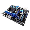
ASUS M5A99X EVO AM3+ Review
BIOS Walkthrough »The Board - A Closer Look


Our usual first item to look at, of course, if the BIOS chip itself, which in this instance, is supplied by Winbond. Nestled securely in a socket that makes user replacement fairly simple, the M5A99X EVO shows that user experience is first and foremost with ASUS. Once the BIOS has booted the M5A99X EVO up, the real brains of the board, the EPU and TPU chips, are in full operation. We've covered these specific parts in our P8P67 PRO and M5A97 EVO reviews before, and the exact same parts are here on the M5A99X EVO. The second picture shows the EPU/DIGI+ chip, located right above the socket near the board edge, with the TPU chip located just under the southbridge. Offering full customization of the board's VRM, from current capabilities, to even the frequency the VRM operates at, this combination is something we were surprised to see here, yet because our testing has proven that this solution is one of the best out there, it was most definitely a pleasant surprise.


There are several switches placed around the board; the MemOK! switch is aptly located to the right of the DIMM slots, and the TPU and EPU switches are found on the board's bottom edge, for easy access when multiple expansion cards are installed. The MemOK! switch, when depressed, will start a boot-up routine that will test the installed memory, and then boot the board with stable voltages and timings, allowing users not only to get into the BIOS to revert from bad settings, but also allowing users to save the settings suggested by the MemOK function. The EPU switch offers automatic power profile adjustments focused on lowering overall board power consumption, while the TPU does the exact opposite, providing an easy way for users to overclock their system, with settings that have been extensively tested to provide full stability with the majority of CPU and memory on the market today. As always though, there is no guarantee that the settings will be 100% stable, so if you do happen to use this feature, be sure to properly test for stability after flipping the TPU switch.
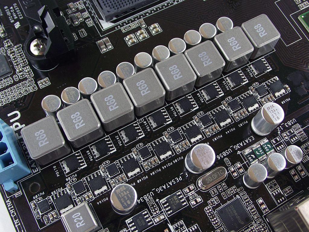


The M5A99X EVO's VRM is controlled directly by the EPU/DIGI+ chip, unlike the Intel boards we looked at previously, with many boards having two engines controlled via the EPU chip. Close examination of the VRM components shows a traditional hi/low MOSFET configuration, with input drivers located next to each MOSFET pair, just like we found on the M5A97 EVO. The dual DIMM phases feature a similar config, with the input driver located next to the MemOK switch. The northbridge VRM is similar as well, employing three MOSFETs like the CPU phases, rather than the two seen in the DIMM VRM. All three VRM sections are controlled by both the TPU and EPU chips, which together create the "Dual Intelligent Processor" technology mentioned on the box front.


Once the board's been powered on, there is a series of four LEDs that light up in succession as the board boots, functioning as a POST code reader of sorts. Should the boot process fail during any of the steps, the LED will remain lit, giving the user a clear indicator as to what part is causing the boot failure; a very useful tool when troubleshooting overclocks.

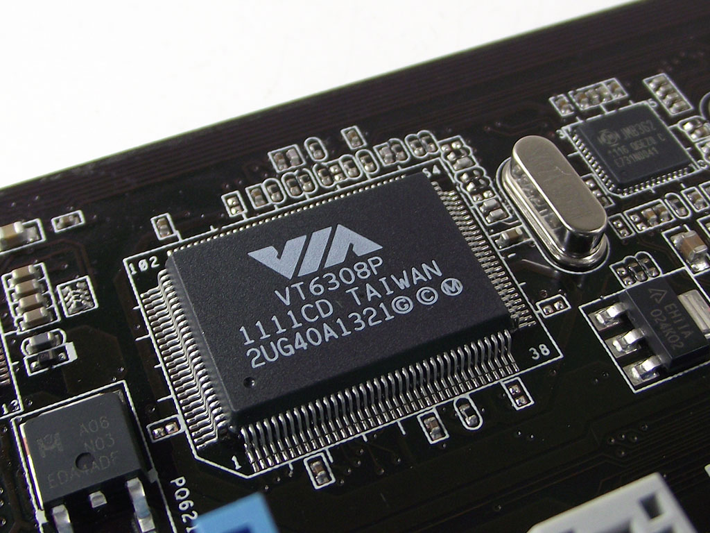
For Super I/O functionality, we find an ITE IT8721F, a part used quite often on other products. As is usual, this chip is responsible for fan control and data monitoring. The VIA VT6308P drives the FireWire port found on the backplane, as well as the internal FireWire port header found near the board's bottom edge.
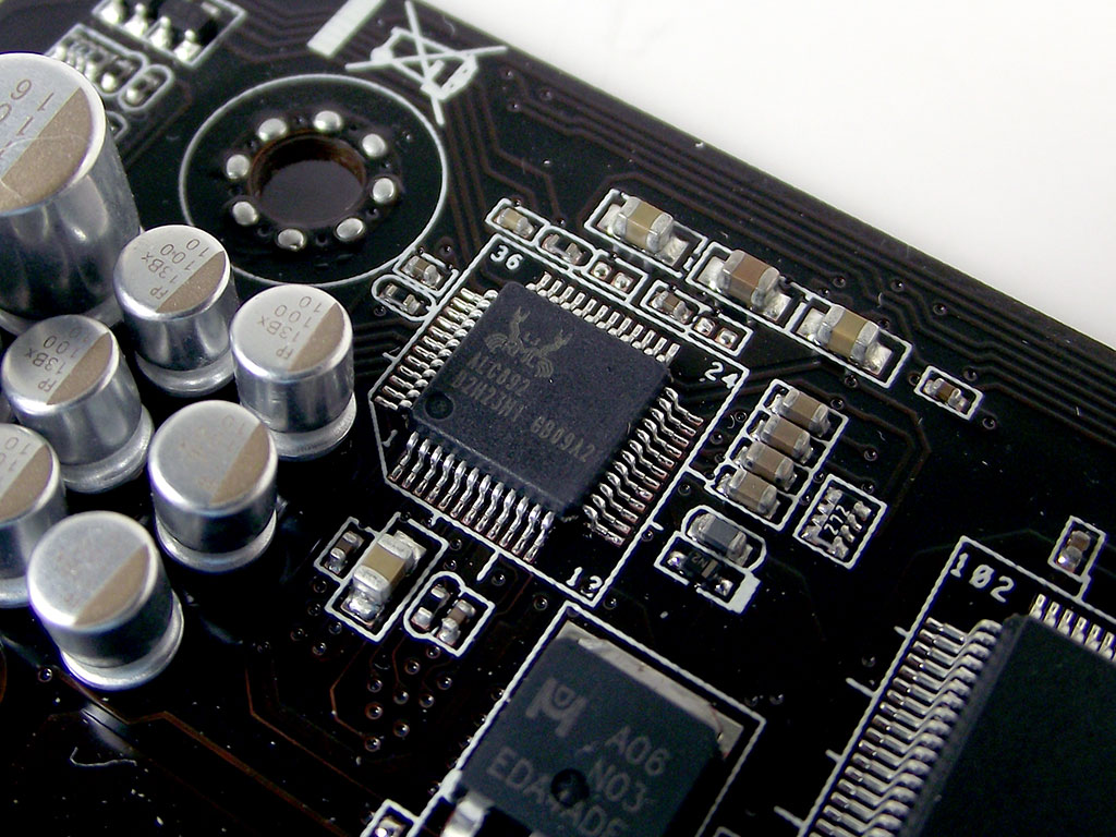
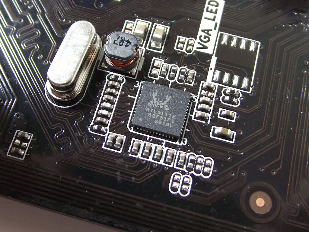
The included Realtek ALC892 HD codec supports 7.1+2 audio, and meets Microsoft's WLP3.x audio requirements. Using DACs that output a 97 db SNR, and ADCs with a 90 db SNR, it supports 44.1k/48k/96k/192 kHz sampling at 16-, 20- and 24-bit, including full support for HD audio formats featuring Content Protection, if supporting software is used. It is also DirectSound 3D compatible, so no area of usage or functionality is overlooked. ASUS has also sourced the LAN controller for the ASUS M5A99X EVO from Realtek; an utterly common RTL8111E PCIe part, located near the board's left edge just under the rear I/O assembly.

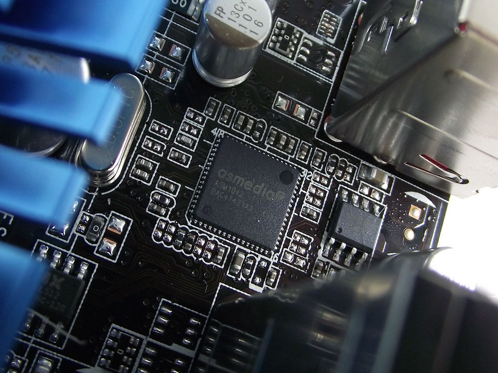
For USB 3.0 support, we find two matching Asmedia AS1042 PCIe controllers, with one under the DIMM slots, supporting the internal port we find nearby the controller itself, while the second is hidden between the VRM heatsink, and the rear I/O assembly. While these controllers are not as familiar as the NEC/Renesas controller, which is far more common, we have found Asmedia controllers to be used on many recently-released ASUS products.


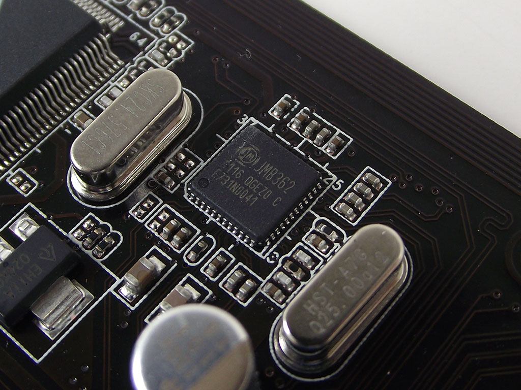
Situated between the PCIe x16 slots we find an ICS clock generator, none other than the ICS 9LPRS477DKL. Specifically designed for the AMD platform, it controls all host clocks, CPU and Southbridge included. The final board components, from JMicron, are both the JMB362 chipset, which provides support for the dual eSATA 3.0 Gb/s ports found on the rear I/O, as well as controlling the dual black SATA 3 Gb/s internal ports we mentioned earlier. Having been on the market for several years, the JMB362 seems to fit in perfectly with what we expect from the ASUS M5A99X EVO, with the extra controller and connectivity being part of what separates the M5A99X EVO from the M5A97 EVO.


For cooling, ASUS has equipped the M5A99X EVO with several blue-anodized aluminum passive heatsinks, which you can see in the pictures above. The Northbridge heatsink is fairly beefy, and the same profile design is carried over to the VRM heatsink as well, with a single heatpipe connecting the two together. The Southbridge heatsink, however, is quite small, providing several millimeters of clearance for installed expansion cards, yet through our testing, proved more than adequate. Upon removal of the VRM/NB heatsink assembly, we noticed near perfect contact from end to end, such that we do hope to see the same thermal interface pad used on other products. You can see clear impressions made by the VRM's components, ensuring that every critical component gets the cooling it needs, extremely vital when it comes to overclocking. The northbridge heatsink uses a gummy pink thermal interface material that pulled away from both the cooler and the northbridge itself when we removed the cooler. This material is such that we recommend that the northbridge cooling is NOT removed under any circumstances, as it was quite difficult to clean off of the northbridge chipset. This also prompted us to not remove the southbridge heatsink; we only removed the northbridge cooler as it was necessary in order to remove the MOSFET cooler, just like the M5A97 EVO.
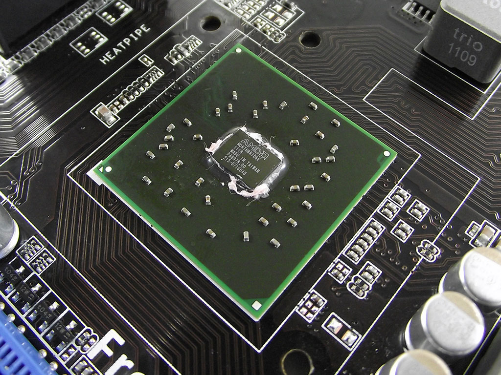
In the above picture you can clearly see the new AMD990X chipset, and as you can tell, it’s very similar to the AMD970 chipset featured in the M5A97 EVO review. The manufacture date listed tells us that we got the final board shortly after ASUS got the chipsets from AMD, as the chip was "minted" during the 18th week of 2011, coinciding with the middle of May. Of course, the major difference here is the chipset’s ability to configure the PCIe lanes into two separate x8 links, for both Crossfire and SLI support.
We're not done yet though; hit the link next page link to take a look at one of our favorite features, the BIOS.
Apr 25th, 2024 05:02 EDT
change timezone
Latest GPU Drivers
New Forum Posts
- Meta Horizon OS (16)
- Core i5-6300U (14)
- (Anti) SFF fun house (351)
- Alphacool CORE 1 CPU block - bulging with danger of splitting? (4)
- The TPU UK Clubhouse (24786)
- Github comments used to push malware via Microsoft repo urls (3)
- Bizarre Throttlestop issue (5)
- GTX 1070 Ti - TDP Issues - Always Power Throttling (5)
- What phone you use as your daily driver? And, a discussion of them. (1471)
- What's your latest tech purchase? (20337)
Popular Reviews
- Fractal Design Terra Review
- Thermalright Phantom Spirit 120 EVO Review
- Corsair 2000D Airflow Review
- Minisforum EliteMini UM780 XTX (AMD Ryzen 7 7840HS) Review
- ASUS GeForce RTX 4090 STRIX OC Review
- NVIDIA GeForce RTX 4090 Founders Edition Review - Impressive Performance
- ASUS GeForce RTX 4090 Matrix Platinum Review - The RTX 4090 Ti
- MSI GeForce RTX 4090 Suprim X Review
- MSI GeForce RTX 4090 Gaming X Trio Review
- Gigabyte GeForce RTX 4090 Gaming OC Review
Controversial News Posts
- Sony PlayStation 5 Pro Specifications Confirmed, Console Arrives Before Holidays (116)
- NVIDIA Points Intel Raptor Lake CPU Users to Get Help from Intel Amid System Instability Issues (106)
- AMD "Strix Halo" Zen 5 Mobile Processor Pictured: Chiplet-based, Uses 256-bit LPDDR5X (101)
- US Government Wants Nuclear Plants to Offload AI Data Center Expansion (98)
- Windows 10 Security Updates to Cost $61 After 2025, $427 by 2028 (84)
- Developers of Outpost Infinity Siege Recommend Underclocking i9-13900K and i9-14900K for Stability on Machines with RTX 4090 (84)
- Windows 11 Now Officially Adware as Microsoft Embeds Ads in the Start Menu (80)
- TechPowerUp Hiring: Reviewers Wanted for Motherboards, Laptops, Gaming Handhelds and Prebuilt Desktops (78)